
Overview
An ideal digital-to-analog converter (DAC) with an output voltage or current that is ideally linear with the input and is immune to other external factors such as temperature. Of course, in practical applications, the DAC is bound to be affected by various external factors, and temperature is an obvious factor. The DAC output will drift with temperature. This is especially important when accurately setting the bias voltage with a high precision DAC. We can calibrate all static drifts, but it is difficult to compensate with temperature changes. Temperature-induced errors are mainly: offset error and gain error.
This application note describes how to determine the offset error, gain error, and temperature of the DAC to help designers anticipate these error factors during the design process. Mastering this knowledge also helps ensure that the system meets specifications in terms of temperature characteristics.
Offset and gain error
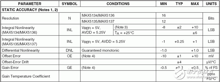
As mentioned above, many error factors can affect DAC performance, such as offset error and gain error. The “Static Accuracy†parameter section of the DAC device data sheet shows the effects of these factors. Figure 1 shows the specifications for the MAX5134 16-bit, 4-channel DAC.
Note 4: Gain and offset test, test point at 100mV and AVDD
Figure 1. Offset and gain error of the MAX5134.
What do these parameters mean for DAC performance?
Offset error usually defines the output of the device at zero crossing. For unipolar outputs, this value is the output corresponding to zero code, usually called zero code error; for bipolar output, the DAC output corresponding to the intermediate code value is defined. .
The gain error is the slope of the transfer function. For the MAX5134, the slope is between 99.5% and 100.5% of the theoretical value.
Figure 2 shows the offset error and gain error. Note that the offset and gain errors can be positive or negative.
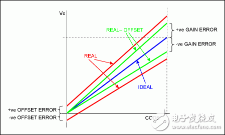
Figure 2 Offset and gain error.
Usually we do not directly measure the offset and gain error. If a unipolar device exhibits a negative offset error, the test result at zero code is obviously incorrect. Because unipolar DACs are typically powered from a single positive supply, the DAC will not produce a negative value. Two points can be tested, and then the offset and gain errors are calculated. One test point is close to zero code, and the other side is close to the maximum code value, even at the maximum code value. For the MAX5134, two test points, 100mV and power supply AVDD, can be selected. See Table 4 for Note 4 (Note 4: Gain and Offset Test, test points at 100mV and AVDD, see the MAX5134 data sheet, available for download from the Maxim website).
Considering the effect of temperature below, both the offset error and the gain error will drift with temperature. For those applications that use the DAC to accurately set the bias voltage, the effect of temperature drift is greater. If the offset and gain errors are fixed, calibration can be performed by a variety of techniques, some of which can be used). In general, temperature drift calibration is a very complicated task, first need to measure the temperature, and then take the corresponding compensation according to the temperature value.
Calculation examples and typical results
Here, taking the MAX5134 as an example, we can get the maximum static error by evaluating the statistics of a large number of devices. We first define several concepts or equations to calculate the error range.
VOUT = N &TImes; G &TImes; (GE + GET) + OE + OET

| Here:: | VOUT = output voltage |
| N = DAC input code value | |
| G = DAC gain | |
| GE = DAC gain error | |
| GET = additional gain error due to temperature change | |
| OE = DAC offset error | |
| OET = additional offset error due to temperature change | |
| VREF = reference voltage | |
| NMAX = DAC maximum code value |
The offset error drift of the parameter is ±4μV/°C, using a box method. In order to determine the temperature offset, you can use the temperature drift coefficient multiplied by the temperature range. Note that the temperature range here refers to the operating temperature range specified by the device, not the actual temperature range. In this example: -40 ° C to +105 ° C, and the temperature-induced offset drift is ±0.58 mV. Similarly, the gain drift coefficient is 2 ppm/°C, which corresponds to ±0.029% FS (full scale).
For the first example, we use a 2.5V reference VREF, which is a 16-bit device, ie the maximum code value NMAX is 65535.
Another problem is the ease of use. It is best to specify the offset and gain error as the "min/max" value, while the temperature effect can only be defined as a typical value. We can estimate changes over the entire range using typical values ​​or empirically, with typical values ​​used here.
The curve shown in Figure 3 is a plot of the relationship between the initial error output voltage and the input code. This is a characteristic curve of an actual DAC device. This set of curves is tighter than Figure 2 and is not easy to analyze. It is best to draw the deviation between them and the ideal curve, as shown in Figure 4. Figure 4 also shows the overall error including the temperature effect.

Figure 3. A plot of the DAC output versus the input code showing the effects of gain and offset error with a reference voltage of 2.5V.
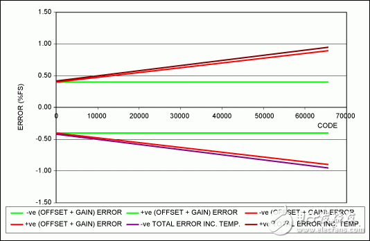
Figure 4. The relationship between the DAC output error and the input code. The reference voltage is 2.5V.
As can be seen from the figure, the effect of temperature is much lower than the initial error, so even if the data sheet only gives typical values ​​of temperature characteristics, it will not have a significant impact on the overall error. The overall error at zero code is ±0.423% FS (±10.6mV) and the overall error at the maximum input code is ±0.952%FS (±23.8mV).
Some improvement measures can be taken, such as raising the reference voltage. Since the gain error is specified as a percentage of full scale (%FS), its absolute value will become larger, but the absolute value of the offset error will not become larger. Therefore, the full-scale output voltage can be increased by increasing the reference voltage, and then the output of the DAC can be externally reduced to the required voltage, so that the gain error is restored to the original value, and the offset error can be reduced. Figure 5 shows the effect of this method.
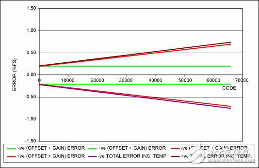
Figure 5. Example of the relationship between the DAC output error and the input code. The reference voltage is 2.5V.
At zero code, the overall error is ±0.212% FS (±5.3mV); at the maximum code, the overall error is ±0.740%FS (±18.5mV).
Of course, this result ignores the error introduced by the output voltage divider. But this method is completely feasible, because the output voltage divider can use a precision voltage divider, such as the MAX5490, which has a temperature accuracy of ±0.05%. Of course, the disadvantage of dividing the DAC output is to reduce the drive capability and improve the output drive through the op amp, which introduces additional errors. An in-depth discussion of this approach is beyond the scope of this article.
in conclusion
This article discusses the offset and gain errors that affect the accuracy of the DAC. It also shows how to calculate the error under worst-case conditions and provides some suggestions for improving the overall error.
In-ear Wired Earphones, they are small and comfortable and simple, fit in just about any pocket,and they provide great sound that literally goes straight into your ears,bring it on your next commute or run, or simply enjoy it in the comfort of your time.
In-ear Wired Earphones
Earbuds With Removable Cable,Earphones With Replaceable Cabl,Stereo In-Ear Earphones,In-Ear Wired Headphones
Dongguang Vowsound Electronics Co., Ltd. , https://www.vowsound.com