
The results of the industry ’s efforts to develop WLAN OFDM products over the past three years have not only reformed the design and verification procedures, but also increased the efficiency of the design by emphasizing initial verification, and thus accelerated the introduction of new OFDM products in the highly competitive consumer market. pace. Zero IF (Zero IF) CMOS RFIC completely subverts the design of WLAN, allowing low-cost products to demonstrate economic benefits. These products usually include fundamental frequency and RFIC, which will integrate some off-chip components, such as power amplifiers, filters and antennas, in the board-level module or package, as shown in Figure 1.
RF and baseband ICs are usually integrated into reference radio prototypes to allow system-level OFDM radio certification testing before mass production of ICs. For example, the use of programmable fundamental frequency IC compensation algorithms can reduce RF IC defects, and these algorithms must be verified during the system-level reference radio test process. The benefit of integrating simulation and verification tools is that WLAN radio system design engineers do not have to wait until later integration to find problems in RFIC or fundamental frequency algorithms, but can verify important OFDM radio specifications early in the design process .
In the integrated design process, RF and baseband IC simulations must be performed at the beginning to verify important specifications before tape-out, thereby shortening the design cycle. During the simulation, various virtual measurements should be performed, that is, the candidate OFDM design should be analyzed to obtain the error vector magnitude (EVM) of the transmitter and debug. The test signal synthesized during the simulation is downloaded to the instrument, and an OFDM test signal can be generated to evaluate the prototype IC. As for the receiver's signal acquisition and bit error rate (BER) testing, it must be performed under signals that include transmitter distortion, channel defects and unwanted interference. To simplify the design process, you can use pre-set test and verification settings to evaluate the design based on the transmitter spectrum, EVM and BER equivalent energy measurement standards.
OFDM radio system
UWB wireless personal network (WPAN) following the IEEE 802.15.3a standard, using a carrier frequency lower than 11 GHz and a data rate of 110 to 480 Mbps to provide short-range (<30 feet) applications, such as wireless in home offices USB and streaming video. The Wireless Metropolitan Area Network (WMAN) that complies with the IEEE 802.16d standard uses a carrier frequency lower than 11 GHz and a data rate of up to 75 Mbps to provide broadband wireless Internet access (BWA) 4 to 6 miles away, or the "last mile" "Internet service. Because spectrum management units, standards development organizations, industrial groups, and various associations are promoting IEEE standards, it is unclear which standards will prevail. It is generally believed that the efforts of various WLAN product manufacturers on the interoperability of consumer products will help the IEEE 802.11a / b / g standard become a global wireless network standard. As for the emerging WPAN / WMAN standard, it will take several years to complete. During the period when various circles are competing to launch new standards, OFDM radio chip designers need flexible design and verification tools to set up new simulation and test solutions in response to different standards.
Accelerate the development of emerging OFDM products
Mixed-signal system integrated single-chip (SoC) verification operations can ensure that the design meets performance specifications based on simulated behavior and component models before IC tape-out and delivery to production. The current 0.1 um IC production process is very long, the cost of the photomask is about 1 million US dollars. SoC designs that contain tens of millions of gates often require hundreds of billions of binary test patterns (test vectors); generating and simulating countless input combinations can ensure that the design will never have an unrecoverable state. The engineering team may spend 50% to 70% of the total design time to perform the verification work. One of the biggest challenges in producing mixed-signal SoCs is that suitable test benches must be developed for analog and digital signals to control and observe internal IC signals during the automated design and verification process. As SoCs become more and more complex, verification during the design cycle becomes particularly important and challenging.
OFDM design engineers integrated the system-level simulation and verification design process to facilitate the early verification of complex IC designs during the simulation process. They also connected the above process with the production process and manufacturing test procedures. In this way, design engineers can use design intellectual property components (IP) throughout the product life cycle to achieve the goal of reducing costs. The following three important strategies can make new OFDM products have higher predictability and profitability:
• Perform preliminary verification
• Integrated design, verification and manufacturing testing
• Perform perfect RF simulation
When the product enters the final stage of development, the impact of design issues on finance and schedule will become more and more obvious. Later integration issues and RFIC's failure to achieve performance goals are the two most common reasons behind project progress and cost exceeding expectations, but can be solved by integrating design, simulation, and test tools and methods. In the development of IEEE 802.11 WLAN OFDM products, several important success factors include:
• Use the OFDM communication model library to perform standard reference radio simulations.
• With reference to the end-to-end simulation and verification of the radio, each system block was developed at a different time.
• When each design team moves individual IP blocks to the next development stage, performance checks are performed.
• Use consistent measurement and analysis algorithms between simulated and physical instruments.
• The design and test stations of different locations and units all use the same performance measurement standards.
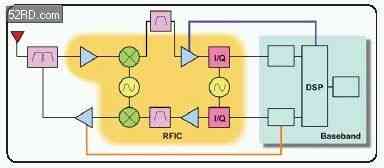
Figure 1. OFDM reference radio.
OFDM product development life cycle
The development life cycle of wireless products begins with the emerging system design specifications and radio structure concepts, and ends with the mass production of profitable products. The pros and cons made at the system level in the beginning determine how to meet important radio system specifications while achieving economical hardware implementation. Carrying out system and circuit level simulations in the design stage can predict in advance whether the proposed wireless structure and related reference radios can meet important specifications. The simulation will use detailed component models, RFIC process design kits (PDK) and RF circuit board / module package parasitics to verify the reference radio against the important performance specifications of each OFDM standard.
Faced with the huge pressure to market quickly, design engineers must use high-efficiency simulation tools to export design IP for reuse in later stages of the life cycle, thereby shortening the design cycle. As radio complexity continues to increase, designers must verify performance as early as possible in the life cycle. In each stage of product performance verification, important problems can be discovered early through simulation to avoid risks. If the problems are corrected later in the development cycle, it may take more time and cost.
Integrated design, verification and manufacturing testing — Connected SoluTIons
Connected SoluTIons combines simulation software and test and measurement instruments to form a variety of flexible solutions. The new design and verification capabilities they provide can be reset in response to different OFDM radio standards. The combination of simulation software and measuring instruments means that you can share signals, measurements, algorithms and data, and only solve special problems that cannot be eliminated by using EDA tools or instruments. The new measurement utility provided by the integration improves the design process and extends the function of the test instrument. In recent years, data communication (as opposed to voice) has greatly contributed to the establishment of wireless communication IC design processes. In the past few years, in the development of various WLAN standards, Connected SoluTIons did meet many flexible verification needs.
The large number of WMAN OFDM subcarriers and the relatively high output power level (relative to WLAN) increase the difficulty of meeting the EVM specifications of power amplifiers / transmitters. Figure 2 uses the ADS advanced design system and Agilent test instruments as an example to design and verify the functional diagram and signal flow of the WMAN 802.16d radio. Download the 802.16d test signal from ADS to the Agilent E4438C ESG signal generator, and then pass the WMAN power amplifier device under test (DUT), and then use the Agilent 89641A VSA vector signal analyzer to analyze to verify the EVM specifications. Figures 3 and 4 show the measurement and simulation results respectively. The measured values ​​are displayed in the VSA display, and the simulation results are displayed in the ADS advanced design system data display format. UWB OFDM frequency hopping makes the design of oscillators and receivers more difficult to meet the requirements of low phase noise and frequency hopping. Figure 5 is a circuit diagram that can generate UWB OFDM Mode 1 frequency hopping (3 frequency hopping); Figure 6 is the simulation result displayed by ADS2004A.
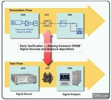
Figure 2. The test bench of WMAN Connected SoluTIons.
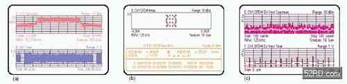
Figure 3. Measured WMAN spectrum (a) spectrum and time, (b) OFDM star chart and symbol / error table, and (c) error vector spectrum and time.
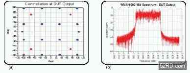
Figure 4. WMAN simulation (a) output star diagram and (b) output spectrum.
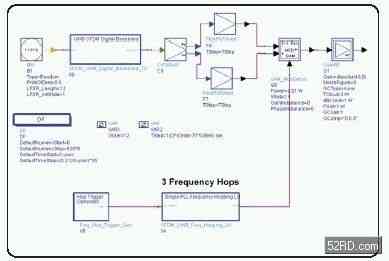
Figure 5. Simulated UWB Mode 1 frequency-hopping signal source.
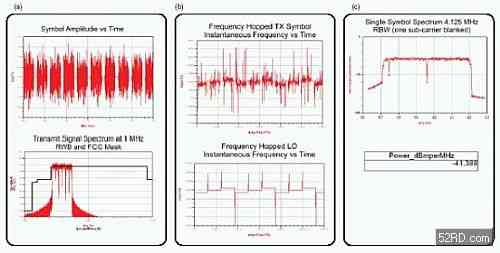
Figure 6. Simulated UWB (a) time burst and spectrum, (b) symbol and LO frequency versus time, and (c) OFDM spectrum.
Move IP to the production stage-use the same algorithm from simulation to testing
In the integrated design and verification process, the design IP of specific OFDM algorithms (developed with design tools such as C, ADS, MatLab (TM), HDL, or VerilogA) can be reused. The ability to quickly move OFDM signals, data, and test vectors between simulation and test operations can help increase the speed of debugging, determine the relationship between test results, and speed up verification procedures. Similarly, IC tester machines can also share the signals generated during the simulation process and shared during manufacturing testing to speed up the development, characterization and contact of production test plans. A well-known mobile phone manufacturer has shortened the connection between the ATE automated test system and the test from a few months to two weeks.
By integrating simulation tools and instruments, you can share the same analysis and verification algorithms in the OFDM design life cycle. Early verification helps shorten the design cycle, because design problems can be detected from the simulation before the IC tape-out, which is absolutely necessary to achieve the ultra-low price target of the OFDM radio chip. At each design stage, system certification tests can be performed in accordance with the emerging UWB and WMAN standards, and in all important stages, automated test benches can be generated and reused for verification. The standardized verification process is suitable for the entire life cycle, so you can seek relevance for the data obtained from the initial design to the production test stage.
Powerbanks are popular for charging smartphones and mobile tablet devices. A powerbank is a portable device that can supply power from its built-in batteries through a USB port. They usually recharge with USB power supply. Technically, a powerbank consists of rechargeable Lithium-ion or Lithium-Polymer batteries installed in a protective casing, guided by a printed circuit board (PCB) which provides various protective and safety measures. Due to its general purpose, powerbanks are also gaining popularity as a branding and promotional tool. Different brands and promotional companies use it as a promotional tool and provide a customized product.
Specifications:
Capacity in mAh: mAh stands for milli Ampere-hour and measures the amount of power flow that can be supplied by a certain powerbank at a specific voltage. Many manufacturers rate their products at 3.7 V, the voltage of cell(s) inside. Since USB outputs at 5 V, calculations at this voltage will yield a lower mAh number. For example, a battery pack advertised with a 3000 mAh capacity (at 3.7 V) will produce 2220 mAh at 5 V. Power losses due to efficiency of the charging circuitry also occur.
Simultaneous charging and discharging: need to specify if the powerbank can be used while it is charging.
Number of output USB ports: This specifies the number of devices that can be charged simultaneously.
Output current rating: This specifies the current rating that it can charge maximum. The higher the number, the better the powerbank. This can vary from output port to output port.
Input Current Rating: Input current rating is the amount of current the powerbank is able to draw at its maximum level while getting charged.
Safety Protections: Over Voltage Protection, Over Charge Protections, Over Current Protections, Over Heat Protections, Short-Circuit Protections and Over Discharge Protections are the common safety measures observed with standard powerbanks.
LED Indications: The Led glows as per indicating the amount of charging ability left with the powerbank.
USB Power Bank,Custom PVC Power Bank,Power Bank Charger,Power Bank Portable Charger
Custom Usb Gift company limited , https://www.customusbgift.com