
Abstract: This application note describes the difference between the primary and secondary termination of a transformer and is commonly used in the signal conditioning link of a pre-high-speed analog-to-digital converter (ADC). This article details the effects of two terminations on the gain flatness and dynamic range of high-speed ADCs in higher intermediate frequency (IF) applications.
The correct selection of input network components is critical to the drive of high-speed ADCs and the balance of input networks (refer to the application note: "Selecting Input Networks Correctly to Optimize the Dynamic Performance and Gain Flatness of High-Speed ​​ADCs").
In higher IF applications, the location of the termination resistor is very important. The AC-coupled input signal can be terminated on the primary or secondary side of the transformer, depending on the system requirements for high-speed ADC gain flatness and dynamic range. A broadband transformer is a commonly used component that can convert a single-ended signal into a differential signal over a wide frequency range, providing a fast and convenient solution. Primary-side termination This article uses MAX1124 (Maxim's recently introduced 250MHz, 10-bit high-IF ADC) as an example to discuss different termination architectures and the impact on high-speed ADC gain flatness and dynamic range. We first take the primary-side termination circuit as an example (Figure 1a). A signal source with an impedance of 50 Ω acts on the primary side of the ADT1-1WT transformer. The secondary side of the transformer is connected to the input filter network of the MAX1124 through a 0.1µF AC coupling capacitor (10Ω isolation resistance + ADC input impedance). The INP and INN pins do not require additional input filter capacitors. In this configuration, the primary side of the transformer can be well matched, and the equivalent ADC input impedance of the secondary side of the transformer is 4kΩ / 3pF. The unbalanced secondary impedance and the leakage inductance of the transformer will form a resonant circuit, producing a gain peak frequency in the frequency range of 450MHz to 550MHz (Figure 1b).
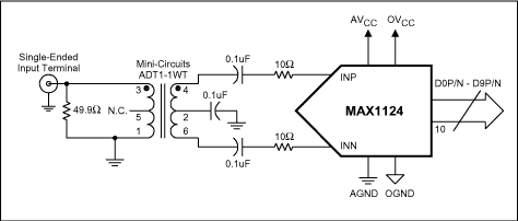
Figure 1a
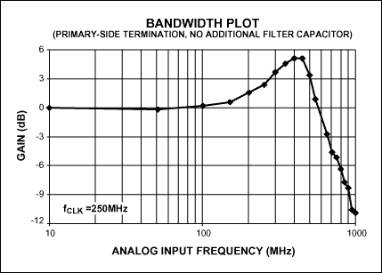
Figure 1b Termination of the secondary side In order to eliminate the gain spike when driving the differential input, we removed the primary termination resistor and used the secondary termination to apply a signal source with an impedance of 50Ω to the ADT1-1WT. In this case, two 25Ω resistors are required for the secondary termination, which are connected between the top / bottom and the center tap (Figure 2a). After the matching resistor is a 0.1µF AC coupling capacitor and input filter network (15Ω series resistance + ADC input impedance), so that a good balanced signal can be obtained on the secondary side, which acts on the input of the ADC. Similar to the configuration in Figure 1, the INN and INP pins have no additional input filter capacitors. This termination method can eliminate gain spikes in the 450MHz to 550MHz band. If necessary, the 15Ω isolation resistance can be replaced with 30Ω to increase the DC attenuation. Although this type of termination can achieve a flatter frequency response, there is a loss of bandwidth (Figure 2b).
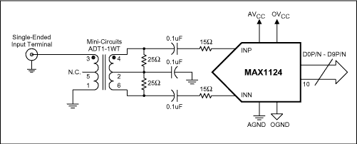
Figure 2a
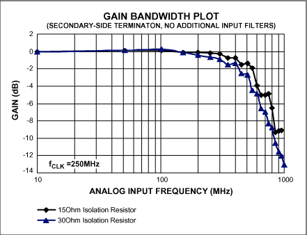
Figure 2b Conclusion This application note discusses the design of high-speed data converter input networks, the rational selection of passive components is very important, and the reasonable use of these components is also important. For example, if the system has very strict requirements for gain flatness, it is necessary to avoid imbalance and resonance at the differential input of the converter to ensure the dynamic index of the system.
In both configurations, no filter capacitors are used at the input, which introduces additional noise at the INP and INN pins. From the simple analysis results, it will reduce the signal-to-noise ratio (SNR) by 0.2dB to 0.5dB. In most high-IF ADC applications, it is critical to ensure gain stability (gain flatness) and dynamic range in a wide frequency range. For a 10-bit resolution data converter, the acceptable noise performance is not obvious. Of deterioration. References MAX1124EVKit Datasheet, Rev0, 11/2003, Maxim Integrated Products, Sunnyvale, CA
MAX1124 Datasheet, Rev0, 11/2003, Maxim Integrated Product, Sunnyvale, CA
Application Note: Correctly select the input network to optimize the dynamic performance and gain flatness of the high-speed ADC
The correct selection of input network components is critical to the drive of high-speed ADCs and the balance of input networks (refer to the application note: "Selecting Input Networks Correctly to Optimize the Dynamic Performance and Gain Flatness of High-Speed ​​ADCs").
In higher IF applications, the location of the termination resistor is very important. The AC-coupled input signal can be terminated on the primary or secondary side of the transformer, depending on the system requirements for high-speed ADC gain flatness and dynamic range. A broadband transformer is a commonly used component that can convert a single-ended signal into a differential signal over a wide frequency range, providing a fast and convenient solution. Primary-side termination This article uses MAX1124 (Maxim's recently introduced 250MHz, 10-bit high-IF ADC) as an example to discuss different termination architectures and the impact on high-speed ADC gain flatness and dynamic range. We first take the primary-side termination circuit as an example (Figure 1a). A signal source with an impedance of 50 Ω acts on the primary side of the ADT1-1WT transformer. The secondary side of the transformer is connected to the input filter network of the MAX1124 through a 0.1µF AC coupling capacitor (10Ω isolation resistance + ADC input impedance). The INP and INN pins do not require additional input filter capacitors. In this configuration, the primary side of the transformer can be well matched, and the equivalent ADC input impedance of the secondary side of the transformer is 4kΩ / 3pF. The unbalanced secondary impedance and the leakage inductance of the transformer will form a resonant circuit, producing a gain peak frequency in the frequency range of 450MHz to 550MHz (Figure 1b).
Figure 1a
Figure 1b Termination of the secondary side In order to eliminate the gain spike when driving the differential input, we removed the primary termination resistor and used the secondary termination to apply a signal source with an impedance of 50Ω to the ADT1-1WT. In this case, two 25Ω resistors are required for the secondary termination, which are connected between the top / bottom and the center tap (Figure 2a). After the matching resistor is a 0.1µF AC coupling capacitor and input filter network (15Ω series resistance + ADC input impedance), so that a good balanced signal can be obtained on the secondary side, which acts on the input of the ADC. Similar to the configuration in Figure 1, the INN and INP pins have no additional input filter capacitors. This termination method can eliminate gain spikes in the 450MHz to 550MHz band. If necessary, the 15Ω isolation resistance can be replaced with 30Ω to increase the DC attenuation. Although this type of termination can achieve a flatter frequency response, there is a loss of bandwidth (Figure 2b).
Figure 2a
Figure 2b Conclusion This application note discusses the design of high-speed data converter input networks, the rational selection of passive components is very important, and the reasonable use of these components is also important. For example, if the system has very strict requirements for gain flatness, it is necessary to avoid imbalance and resonance at the differential input of the converter to ensure the dynamic index of the system.
In both configurations, no filter capacitors are used at the input, which introduces additional noise at the INP and INN pins. From the simple analysis results, it will reduce the signal-to-noise ratio (SNR) by 0.2dB to 0.5dB. In most high-IF ADC applications, it is critical to ensure gain stability (gain flatness) and dynamic range in a wide frequency range. For a 10-bit resolution data converter, the acceptable noise performance is not obvious. Of deterioration. References MAX1124EVKit Datasheet, Rev0, 11/2003, Maxim Integrated Products, Sunnyvale, CA
MAX1124 Datasheet, Rev0, 11/2003, Maxim Integrated Product, Sunnyvale, CA
Application Note: Correctly select the input network to optimize the dynamic performance and gain flatness of the high-speed ADC
Dc Servomotor,Brushless Dc Servo,Small Brushless Dc Motor,200W-400W Dc Servo Motors
Jinan Keya Electron Science And Technology Co., Ltd. , https://www.keyaservo.com