
Keywords: frequency synthesis, principle circuit, design
1 Introduction Frequency synthesizer is the frequency source of modern communication station, also known as excitation source, which can provide high stable working frequency for all working channels of the station. A large-scale integrated phase-locked digital synthesizer controlled by a single-chip microcomputer is used in military and civilian communication radio stations. Due to the use of intelligent microcomputer control technology and digital synthesis technology, the operation of the radio station is greatly simplified and the reliability of the radio station is improved. Sex. This article introduces a pulse swallowed digital frequency synthesis loop. Its core circuit uses a single-chip large-scale integrated circuit MC145156 dedicated for phase-locked loop digital frequency synthesizer and a dual-mode prescaler integrated circuit SP8793. Its main features are higher working frequency band, less output clutter and noise interference, simple circuit and reliable operation.
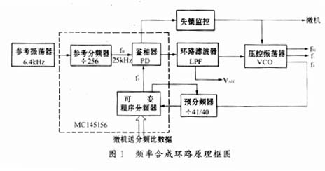
2 Circuit composition and principle The digital frequency synthesis loop is mainly composed of integrated phase-locked synthesizer, prescaler, reference oscillator, loop low-pass filter and voltage-controlled oscillator. Its circuit structure is shown in Figure 1. .
The microcomputer inputs the frequency-dividing data corresponding to the working frequency f0 into the variable program frequency divider, and controls the variable program frequency divider and the pre-frequency divider to divide f0 frequency N times at the same time, fv = f0 / N = 25kHz, fv Phase comparison with the standard signal frequency fR in the phase discriminator, the resulting phase error voltage passes through the loop low-pass filter to control the VCO, so that the output f0 frequency is stable. When the error Δθ between the phase θv of the fv signal and the phase θR of the fR signal is within the synchronous band of the phase-locked loop, the loop is trivial, and the error voltage output by the PD always tracks the change of θv to control the VCO, so that fv = fR, f0 = N fR, that is, the frequency is fixed so that f0 and fR have the same frequency stability. When f0 changes greatly and fv deviates more from fR, the phase error Δθ of the two exceeds the loop capture band, which will cause the loop to lose lock, fv ≠fR, and f0 frequency is out of control. At this time, the PD outputs a lock-out monitoring signal The VCO is controlled by the loss-of-lock monitoring control circuit to stop transmitting the excitation output and notify the microcomputer to issue a loss-of-lock alarm.
3 Circuit design
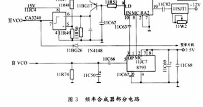
3. 1 VCO circuit Voltage controlled oscillator VCO is a radio frequency source, it is a voltage / frequency conversion component, the oscillator frequency is controlled by the error voltage output by the phase discriminator through phase negative feedback, and its output frequency stability is high. The oscillator circuit of VCO is composed of two electric field effect tubes 10BG7, 10BG8 and four varactor diodes 10BG3, 10BG4, 10BG5, 10BG6 and inductance 10L1, as shown in Figure 2. The four diodes are connected in series to improve the voltage and capacitance control characteristics. The static reflection bias generated by the regulator 10BG2 and the control voltage VC sent by 10JC1 via 10BG1 are superimposed on 10R5, which is added to the negative electrode of the varactor diode by 10R7. . When VC increases, the equivalent capacitance of the varactor decreases correspondingly, which increases the loop resonance frequency, that is, the VCO oscillation frequency, and vice versa. 10BG7 is a common source connection method, 10BG8 is a common gate connection method, and they form a three-point inductive oscillator with the oscillation circuit, and 10C9 and 10L1 form a positive feedback circuit. The oscillation voltage is coupled out from the 10BG7 drain through 10C11.

3.2 Reference Oscillator and Reference Frequency Divider The reference oscillator uses the 6.4MHz frequency generated by the external crystal oscillator 11JST1 as the reference frequency. The circuit is shown in Figure 3 and is input from pin 19 of 11JC6. The NOT gate is added to the reference divider. 11JST1 potentiometer 11W2 can fine-tune the frequency of the oscillator. At the same time, the crystal signal of 6.4MHz is output from the 18th pin of 11JC6 and sent to the clock circuit of the single-chip 11JC8.
According to the international aviation general standards, the minimum frequency interval of the radio frequency synthesizer output radio frequency is generally 25kHz, therefore, the reference reference frequency fR should also be 25kHz, the reference oscillator signal frequency is 6.4MHz, the reference frequency division ratio R = 6.4MHz / 25kHz = 256 times. The corresponding address code is 011, so the RA2 (2) terminal of 11JC6 is grounded, and both RA2 (1) and RA0 (20) terminals are connected to + 5V. The 25kHz reference frequency fR signal is sent to an input of the on-chip A phase detector.
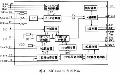
3.3 Integrated phase-locked loop circuit This synthesizer uses a dual-mode phase-locked loop CMOS integrated circuit (MC145156), as shown in Figure 4 for the internal circuit structure of MC145156, which contains the reference oscillator frequency divider, A And B digital phase detector, 10-bit ÷ M counter, 7-bit ÷ A counter, 19-bit serial code input shift register and latch, prescaler variable-mode logic control and lock detection, etc. Use with prescaler. Its main features are: 20-pin dual in-line package; reference frequency division ratio R = 8, 64, 128, 256, 540, 1000, 1024, 2048; program divider count range is M = 3 ~ 1023, A = 0 ~ 127; phase detector A is a single-ended three-state output: Kd = VDD / 4π (V / rod); phase detector B is a double-ended output: Kd = VDD / 2π (V / rod). The circuit connection relationship is shown in Figure 3.
3.4 Prescaler and program divider The dual-mode prescaler is an integral part of the pulse swallowing variable divider, and its circuit structure is shown in Figure 3. The dual-mode prescaler is a special-purpose integrated circuit SP8793 (product of British Plessey company), which is a high-speed low-power digital integrated circuit using the ECL process. Its main performance is: the highest operating frequency of 225MHz; the dual-mode frequency division ratio of ÷ 40/41, the mode control MC is 41 when the power frequency is low, and the MC is the high frequency division ratio is 40. The f0 voltage SP8793 from the VCO is input from the 5th pin, after being divided by ÷ 40/41, it is output from the 3rd pin, from the 10th pin of the MC145156 to the program divider, the MC signal from the program divider is from the 8th pin of the MC145156 Pin 1 output to SP8793 controls its frequency division mode.

The program divider is integrated inside MC145156, and is composed of 10-bit M counter and 7-bit A counter, which are programmed by 10-bit binary and 7-bit binary codes respectively, corresponding to M = 3 ~ 1023 and A = 0 ~ 127, M, A The preset of the value is completed by the microcomputer control. The frequency division process is that when the f0 output by the VCO is input into the dual-mode prescaler, under the control of the MC145156 internal circuit MC signal output by the MC145156 control logic, it is predivided by ÷ 40/41 Frequency and input into the program divider for ÷ A, ÷ M frequency division counting, the generated N-time frequency division signal fV is sent to the on-chip A phase detector and compared with the reference frequency fR to generate an error control signal to track the f0 Change, when the loop is locked, fV = fR, f0 = NfR. It can be seen that the output frequency of the VCO can be changed by changing the M and A values ​​of the pulse swallowing variable frequency divider.
3.5 Loop filter The loop filter circuit is composed of an integrated operational amplifier 11JC5 and some resistors and capacitors to form an active second-order proportional integral filter, as shown in Figure 3, the operational amplifier is connected into a differential working mode, phase detection The ФV and ФR error voltages output by the amplifier are respectively passed through two symmetrical RC proportional integral filter circuits, which are added to the non-inverting and inverting input terminals of the op amp. resistance. The filtered control voltage VC is output by pin 6 of 11JC5 and sent to the VCO.
3.6 Loss of lock detection control circuit The function of the loss of lock detection control circuit is to send out the loss of lock information to the microcomputer when the frequency-locked phase loses lock and make the display circuit alarm; if the radio station is in the transmitting state, the VCO must The RF amplifier does not work, the output of the RF excitation is stopped, and the detection of the lockout monitoring information is completed in the MC145156 chip.
4 Conclusion The circuit technology of the synthesis loop has basically realized integration and digitization, and the advanced technology level has been proven by many tests and practical applications. The circuit has the characteristics of high frequency bandwidth, high stability, simple circuit and low cost, and easy operation and use. The synthesizer can be used as a frequency source for communication stations as well as a frequency source for measuring instruments, and has certain promotion and use value.
references
2 Edited by Yanli and Wangyou Village. Modern communication system. Beijing: Electronic Industry Press, 2001
3 Edited by Zhou Jie and others. Ultrashort wave air-to-air communication equipment. Published by Naval Aeronautical Technology College, 1996
Tongchai Diesel Generator,Tongchai Diesel Generator Set,500Kva Tongchai Diesel Generator,500Kva Tongchai Diesel Generator Set
Jiangsu Lingyu Generator CO.,LTD , https://www.lygenset.com