
At present, the tire pressure monitoring system TPMS (TIre Pressure Monitoring System) for automobile safety is gradually entering the market, becoming the standard configuration in automobiles, and playing an irreplaceable role in protecting the life safety of drivers and pedestrians.
In the active TPMS, the monitored pressure, temperature and other data need to be transmitted to the console in real time. The pressure monitoring module is usually installed on the valve or on the wheel hub with a buckle, so the data monitored by these two installation methods can only be transmitted to the receiving device in the cab through wireless communication in order to remind the driver in time Pay attention to changes in tire pressure to avoid possible accidents.
In the actual use of TPMS, it is impossible to frequently remove the tire to replace the battery of the transmitter module, so it is necessary to achieve the same life of the pressure monitoring module and the tire. This puts very strict requirements on the power consumption of the transmitting module, which requires not only the maximum transmission power as possible, but also the ability to transmit the signal to the receiving end in time and accurately; and the energy required for transmission is as small as possible and less It consumes battery energy and prolongs the service life of the transmitter module accordingly. In this way, it is required to select a chip with high emission efficiency as much as possible in actual design, and the fewer peripheral interface circuits, the better, and comprehensively reduce the system power consumption in many ways.
Due to the harsh operating environment in the tire, it causes many difficulties for signal transmission and reception, which requires high parameters such as power consumption and temperature of the chip. At present, the manufacturers that can provide such wireless transmitting and receiving chips in the market mainly include companies such as MAXIM, ATMEL, Infineon, and freescale. According to the actual use needs, the factors of power consumption and anti-interference of several types of products are comprehensively considered. This design Choose Infineon's transmitter chip TDK5110 and receiver chip TDA5210, and sensor chip choose Infineon's SP12.
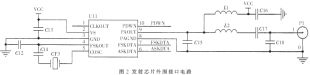
1 Launch chip circuit design
The working frequency band of the single-chip ASK / FSK transmitting chip TDK5110 is 433MHz-435MHz, which is the ISM (Industrial ScienTIfic Medical Band) frequency band. The TDK5110 integrates a PLL and has an efficient power amplifier to drive the transmitting antenna. The operating temperature range of the chip is -40 ~ 125 ℃, the power supply voltage range is 2.1 ~ 4V [2], which fully meets the temperature and temperature requirements on car tires voltage range.
TDK5110 provides two data modulation methods, ASK and FSK. ASK is very susceptible to noise interference. FSK is superior to ASK in terms of anti-interference, and the special operating environment where tires are located is subject to a lot of interference. So this design uses FSK's data modulation method. TDK5110's chip mainly includes transmit power amplifier (PA), crystal oscillator (OSC), voltage controlled oscillator (VCO), phase detection (PD) circuit, frequency divider, loop filter (LF), FSK switch, etc 2]. The peripheral components of the chip are fewer, which is conducive to the reduction of system cost, and also facilitates the parameter setting and debugging of the system.
In this design, the center frequency of the transmitting chip is 434MHz, and the external crystal oscillator of 13.56MHz is used, and 434MHz is obtained by 32 times the frequency of the phase-locked loop. The choice of transmitting antenna can be either a single-ended antenna or a PCB printed antenna. Since the weight of the entire transmitting module is limited in the tire, it is best to choose a PCB printed antenna. In order to obtain good performance, the area enclosed by the antenna ring should be as large as possible when designing the circuit board. The closer to the edge of the ring, the higher the field density, so the shape of the design is approximately a square [6].
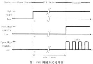
TDK5110 provides three power modes: Low Power Mode (Power Down Mode), PLL Enable Mode (PLL Enable Mode) and Transmit Mode (Transmit Mode) [2]. In low-power mode, the entire chip stops working, and the typical value of current consumption is 14nA at 85 ° C; in PLL enable mode, the PLL starts to work and the power amplifier (PA) does not start, the PLL startup time depends mainly on The size of the external crystal oscillator is generally less than 1 millisecond, and the current consumption is 4mA; in the launch mode, all parts of the chip begin to work, and the typical value of current consumption is 14mA. Of course, in the actual use process, the chip is in low power mode most of the time, even when the car is driving, the data is also intermittently transmitted. So you can set some sending modes and the frequency of data transmission through the software, in order to effectively reduce the power consumption of the system. This design uses the data modulation method of FSK, so according to the timing logic diagram of FSK modulation shown in Figure 1, the peripheral circuit connection of the entire chip is shown in Figure 2. Among them, CLKOUT is a clock signal synchronized with the microcontroller, FSKDATA is a signal connected to the TXD pin of the microcontroller, and the PDWN and ASKDATA pins are connected to the two I / O pins of the microcontroller, and the data transmission mode can be controlled by software .
2 Receive chip circuit design
The receiving chip corresponding to TDK5110 is TDA5210. TDA5210 is a low-power single-chip FSK / ASK superheterodyne receiving chip, working in the 810MHz-870MHz and 400MHz-440MHz frequency bands of ISM. The chip is highly integrated and requires fewer peripherals, which is beneficial to the user's design. There are low-noise amplifier (LNA), double-balanced mixer (mixer), voltage-controlled oscillator (VCO), phase-locked loop (PLL), crystal oscillator, limiter, and FSK demodulation in this chip Circuit (PLL FSK demodulator), data filter (data filter), data slicer (data slicer), peak detector (peak detector) and other circuits [3].
The receiving end selects the FSK data modulation method. At this time, the current consumption is 5.9mA, the receiving sensitivity is -100dBm, and the current consumption is 50nA in the low power consumption mode.
The receiving antenna selects a whip antenna, its length is λ / 4 (λ is the wavelength of the received signal), and the frequency of the received signal is 434MHz, so the length of the antenna is about 17.3cm, and the antenna receives the signal very sensitively. After the signal is received through the antenna, it enters the LNA (low noise amplifier) ​​through an LC filter and amplifies a weak signal. Because the LNA itself has noise, it needs to be filtered by the second LC filter network, and then enter the mixer, and the crystal oscillator is mixed with the frequency of the phase-locked loop frequency-multiplied signal, and the mixed signal passes through the intermediate frequency filter (IF filter ) Enter the limiter. Then pass the digital filter and data limiter to the single chip microcomputer for further decoding processing. The microcontroller at the receiving end selects the 78F0034 microcontroller from NEC [7]. The peripheral interface circuit of the receiving chip is shown in Figure 3. 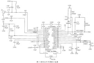
LNA is mainly to amplify the weak signal received by the antenna. The ideal amplifier hopes to only amplify the amplitude of the desired signal without amplifying any distortion signal and noise signal, but in fact the signal inevitably generates noise when passing through the LNA. This requires adding a filter network before and after the LNA. If the parameters are matched properly, the received clutter can be effectively filtered out and the signal-to-noise ratio can be improved. 
The receiver needs to receive data information from four wheels at the same time. How to distinguish which tire the data information comes from needs to be numbered. Infineon's sensor chip SP12 codes a unique serial number for each sensor, which makes it possible to determine the position of the tire by first reading the serial number of the sensor when extracting the relevant information of each sensor [1].
3 System software design
After the system starts, read the in-tire pressure, temperature, battery voltage and acceleration measured by the sensor chip through the single chip microcomputer in the transmitter module, and then send this information and the serial number of the sensor through the transmitter module TDK5210. The data transmission between the sensor chip and the single-chip microcomputer is mainly accomplished through the SPI bus protocol [1].
After the car is started, the receiving end is powered on and starts working. By receiving the relevant data information transmitted from the transmitting end, the pressure change in the tire is monitored in real time. When the pressure is lower than a certain set threshold, the driver is reminded by alerting to take corresponding measures.
The problem of wireless data transmission in the tire pressure monitoring system is a key part of the entire TPMS system. This design has achieved the expected results under laboratory conditions. Because the actual environmental conditions are far more complicated than the laboratory, it needs more experiments and on-site debugging to be used in actual production, and some adjustments and improvements are made on this basis.
Fast Recovery Diode (FRD) is a kind of semiconductor diode with good switching characteristics and short reverse recovery time. It is mainly used in electronic circuits such as switching power supply, PWM pulse width modulator and inverter, as high frequency Rectifier Diode. Use for freewheeling diodes or damper diodes. The internal structure of the fast recovery diode is different from that of a normal PN junction diode. It belongs to a PIN junction diode, which adds a base region I between the P-type silicon material and the N-type silicon material to form a PIN silicon wafer. Since the base region is thin and the reverse recovery charge is small, the reverse recovery diode has a short reverse recovery time, a low forward voltage drop, and a high reverse breakdown voltage (withstand voltage value).
Fast Diode,Fast Recovery Rectifier Diode,Fast Recovery Diode,Fast Switching Diode
Dongguan Agertech Technology Co., Ltd. , https://www.agertechcomponents.com