
Overview This article provides a reference design for a low-jitter clock source for high-speed data converters. The goal is to achieve edge-to-edge jitter <100fs at clock frequencies up to 2GHz. For the 1GHz analog output frequency, the resulting jitter signal-to-noise ratio SNR is: -20 × log (2 × π × f × tj) = -64dB.
Design requirements The maximum frequency of the clock design is 2GHz. However, some VCOs (voltage controlled oscillators) and prescalers can be extended to higher frequencies, and the range that different devices can extend is not the same. The reference design, simulation tests and results presented here are only for the 2GHz output frequency.
Some high-speed converters use both edges of the clock signal as internal timing. This requires a strict 50% duty cycle. In addition, the target output drive capability is 10dBm / 50Ω, which is the 2VP-P differential output.
Synthesizer design basics
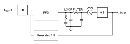
Figure 1. Traditional phase-locked loop
The simplest design is a traditional phase-locked loop circuit, as shown in Figure 1. As mentioned above, a strict 50% duty cycle is required. Therefore, the VCO works at twice the frequency of the target clock (4GHz), and then obtains the target frequency and duty cycle by dividing by 2. Since the frequency divider introduces jitter, it is placed in a phase-locked loop loop to eliminate noise.
The loop filter provides low-pass filtering of reference noise and high-pass filtering of VCO noise. At the same time, it also determines the loop establishment time. Since this is a fixed frequency application, there is no problem with the loop settling time; the filter bandwidth can only be optimized for noise. Narrowband filters are easier to handle reference noise, but increase the noise burden of the VCO, and the effect of wideband filters is the opposite.
Although we need to balance between the VCO and the reference clock, research on both shows that it is possible to obtain the best performance of both. The phase noise index of 100fs jitter determines how low the noise will be.
Phase noise is an index relative to the carrier frequency and inversely proportional to the frequency deviation (dBc / Hz). The set of all phase noise is the phase noise power, which is used to compare with the fundamental frequency power. The phase noise is divided by the fundamental frequency power to obtain jitter.
For example, suppose a 2GHz VCO has an SSB (single sideband) phase noise of -110dBc / Hz from 10kHz to 100kHz, and its bandwidth is 90kHz, resulting in 49.5dB. Therefore, the total noise is -60.5dBc. The SSB noise power is:

Therefore, the effective value of the noise voltage is:

The factor 2 in the root sign represents the inclusion of two single sidebands¹.
Its jitter is:

Equation 3 only yields jitter at a frequency offset of 10kHz to 100kHz. In order to determine the overall jitter, the remaining frequency offset must also be considered.
Another method is that we reverse phase noise from jitter. So, for 100fs jitter at 2GHz:

The SSB noise power is:
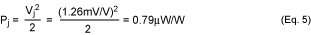
The result of Equation 5 is equivalent to the total noise power (SSB) of -61dBc. If it is assumed that the phase noise is evenly distributed from 1 Hz to 10 MHz, then, converted to dBc / Hz, the following phase noise template is obtained (Figure 2).
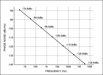
Figure 2. Phase noise template
There is no doubt that jitter <100fs at 2GHz is a very good phase noise value, especially in the range of 10kHz to 100kHz. It can be seen from the figure that the phase noise at 10kHz is approximately -114dBc / Hz. But very few separate VCOs can achieve this level. Of course, it is difficult to achieve this goal with integrated VCOs. UMC (Universal Microwave CorporaTIon) VCO can achieve this low noise level. The bandwidth of UMX series products is 500MHz to 5GHz, and its 10kHz phase noise can reach below -112dBc / Hz. Even the worst VCO in the UMX series meets our requirements.
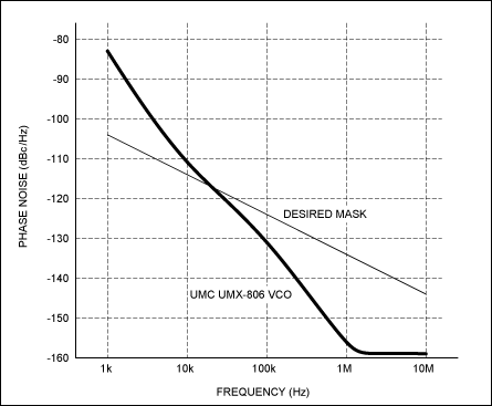
Figure 3. UMX-806-D16 corresponds to the phase noise of the phase noise template
Figure 3 shows the worst-case phase noise of the 4GHz VCO (UMX-806-D16) and our target phase noise template. The phase noise of the VCO below 20kHz is very high, but by designing the bandwidth of the phase-locked loop filter, low-frequency partial VCO noise can be suppressed. Assuming that there are no other factors, a good phase noise index above 10kHz can be obtained. Please note that these phase noise requirements come from a 2GHz oscillator. However, Figure 3 shows the curve of the 4GHz oscillator, which requires an additional divide by 2 to ensure a 50% duty cycle. Assuming that the frequency division by 2 itself does not affect the total phase noise, the phase noise of the VCO will be reduced by 6dB, and the entire curve will shift down by 6dB in parallel.
Note that the reference clock also generates noise, but most of it is distributed below the loop filter bandwidth. Figure 4 shows the Bert diagram of Crystek® 80MHz crystal voltage controlled oscillator and the target phase noise template. Note that the frequency gain of the phase-locked loop will amplify the phase noise of the reference clock in equal times. Therefore, for 80MHz crystal and 2GHz output, the gain is 25. As a result, the Crystek curve will shift up 28dB. This translation means that the phase noise of the reference clock is very high at 1kHz³. However, the phase noise template assumes that the total noise power is evenly distributed within the frequency offset. Of course, this is not necessarily the case, so constant phase noise outside 1kHz plus noise within 1kHz can still meet our jitter specifications.
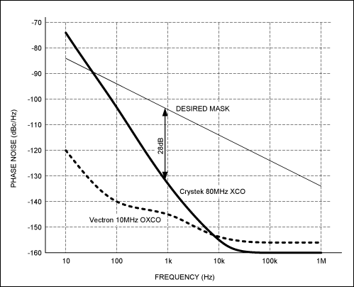
Figure 4. Phase noise of the reference clock
The phase noise analysis in Figure 4 also includes a Vectron constant temperature controlled oscillator (OCXO), which has extremely low phase noise. Note that OCXO easily consumes more power (up to the watt level).
Synthesizer Schematic Figure 5 is the complete circuit schematic of the reference clock and VCO discussed earlier. The PLL uses Fujitsu® MB15E06SR, which integrates a 4mA charge pump and a prescaler up to 3GHz. Because the PLL needs to be programmed, we have adopted a very simple PIC microprocessor (PIC18F2455) with a built-in USB interface that can automatically perform programming tasks. This design requires software to program the user interface, as well as PIC.
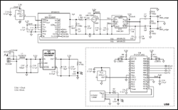
Clear picture (PDF, 93.8KB)
Figure 5. Schematic diagram of the clock synthesizer
The frequency divider uses HitTIte® HMC361, which can work up to 10GHz, and its phase noise has little effect on performance. However, the output swing of the crossover is only 0.8VP-P, or 2dBm at 50Ω. The design goal is 10dBm output (2VP-P), so the output of HitTIte cannot meet the requirements, and the voltage needs to be increased. On Semiconductor® or Zarlink® have similar products, but their output swings are basically the same as HitTIte, or even worse. Moreover, their noise specifications are not clearly marked.
A simple transformer can be used to increase the swing of a low-speed clock, but transformers above 2GHz that can achieve 4: 1 amplification are not common. In addition, this approach increases the difficulty of impedance design. Another method is to use active amplifiers, which can obtain many differential amplifiers with bandwidths> 10GHz, but the noise specifications of the device need to be further determined to meet the design requirements. Another question is whether the amplifier can be placed in the PLL. Fujitsu data sheets recommend a maximum prescaler input of 2dBm (1VP-P).
Simulation results ADIsimPLL (written by Applied Radio Labs for Analog Devices) can be used to analyze the circuit, which includes multiple UMC VCO models. Figure 6 shows the PLL phase noise Bert diagram composed of UMC 4GHz VCO without frequency divider and Crystek oscillator. Below 2kHz, the noise of the reference clock dominates; above 2kHz, the phase detector phase noise dominates; above 70kHz, the VCO noise dominates.
Fig. 6 includes the target noise template (thick black line) of Fig. 2. Obviously, the total noise exceeds the template below 50kHz, which will produce 200fs of jitter. There is a problem in actual simulation, that is, how to solve the phase noise of the phase detector. It should be equal to the noise floor of a particular device (-219dBc / Hz) multiplied by the VCO / PFD frequency, which is 4000MHz / 25MHz, or 44dB, shifted 118dB. Further verification is required, but even if the PFD (Phase Detector) noise is removed, the result is still unacceptable (167fs).
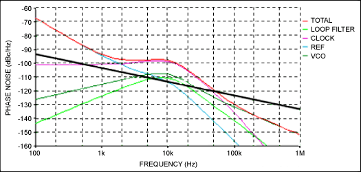
Figure 6. Simulation results using VCO: phase noise at 4GHz
In addition to PFD noise, the filter setting is close to the VCO noise peak at 10kHz. The main remaining problem is the reference clock noise. Unfortunately, the performance better than the template above 40kHz is not enough to eliminate this noise. Therefore, other types of oscillators need to be used to meet the phase noise requirements, such as: OCXO.
The Printed Circuit Board (PCB) of this design can be adapted to three or four different XO pinouts. Figure 7 shows the simulation results using Vectron OCXO. Even considering the phase detector noise, the final jitter is 86.5fs. This jitter leaves a certain margin for the crossover noise that is not considered (the noise should have no significant negative effects) and the amplifier that may be needed.
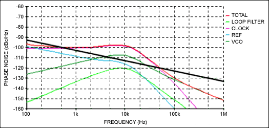
Figure 7. Simulation results using Vectron OXCO: phase noise at 4GHz
Conclusion The jitter target of 100fs at 2GHz is more difficult to achieve than we expected. Experimental data shows that using some standard PLL circuits can achieve this goal. The key lies in the choice of VCO and reference clock. Experiments show that UMX's VCO has first-class phase noise performance. The remaining two problems are: (1) select a reference clock with sufficiently low noise; (2) select a suitable amplifier. Fortunately, we have many devices to choose from, and the same circuit layout can be applied to different types of pin arrangements. The choice of amplifier is more difficult, and further analysis is needed to determine whether it can be placed in the loop, and the impact of its noise needs to be considered.
¹Considering two single sidebands, the factor 2 is included both inside and outside the radical. The total noise power is twice the SSB noise power, so the total noise voltage should be equal to the SSB noise voltage.
² refers to a single component, not a module.
³High phase noise around 1MHz, but the loop filter helps to attenuate this noise.
Rigid PCB , the largest number of PCB manufactured
What is Rigid PCB - Rigid PCB Definition
Rigid PCB is a kind of printed circuit board, and is the largest number of PCB manufactured. It is made of solid substrate material, which can effectively prevent the distortion of the circuit board. Perhaps the most common rigid PCB is the computer motherboard. The motherboard is a multi-layer PCB designed to distribute power from the power supply while allowing communication between all components of the computer, such as CPU, GPU and RAM.
Rigid PCB can be used in any position where the PCB itself needs to be set to a shape and maintained during the remaining life of the equipment. Rigid PCBs can be anything from simple single-layer PCBs to eight or ten-layer multi-layer PCBs.
Rigid PCB and Flexible PCB are totally different. One is flexible and the other is rigid. Therefore, their application scenarios are different. In addition, there are Rigid Flex PCB . There are similarities between them. However, all rigid PCB have single-layer, double-layer or multi-layer structure, so they have common application scope. This is the case.

Some characteristics of rigid PCB
- Rigid PCB is a kind of conventional PCB, which can not be like flexible PCB, because rigid PCB can not be twisted or folded into any shape, because it has FR4 reinforcement, which is very useful for increasing stiffness.
- Rigid PCB is made up of copper trances and paths which are incorporated on a single board in order to connect the different components on the board. The base material of the board is made of rigid substrate which gives rigidity and strength to the board.
- The computer motherboard is the best example of a rigid PCB with a rigid substrate material.
- Once rigid PCBs are manufactured, they cannot be modified or folded into any other shape.
- Rigid PCB is cheaper than flexible PCB. They are traditional PCBs and are widely used in many electronic products.
- Flexible PCB and rigid PCB have their own limitations and advantages in terms of ease of use and availability. Both of them are used to connect multiple electronic components on circuit boards.
Rigid PCB Manufacturing
Rigid PCB is made up of different layers that are joined together using adhesive and heat, providing a solid shape to board material. Following layers are used to develop a rigid PCB.
Substrate Layer - rigid PCB material
- Substrate layer, also referred base material, is made of fiber glass.
- The FR4 is mostly used as a substrate material which a most common fiber glass that provides rigidity and stiffness to the board.
- Phenilcs and epoxies are also used as a base material but they are not as good as FR4, however, they are less expensive and feature unique bad smell.
- Decomposition temperature of phenolics is too low that results in delamination of the layer if solder is placed for long duration of time.


Multilayer Rigid PCB Stackup
Copper Layer
- On the top of substrate layer, there resides a copper foil which is laminated on the board with the help of added amount heat and adhesive.
- In common use, both sides of the board are laminated with copper, however, some cheap electronics come with only one layer of copper material on the board.
- Different boards come with different thickness which is described in ounces per square foot.
Solder Mask Layer
- Solder Mask Layer houses above the copper layer.
- This layer is added on the board to add insulation on the copper layer in order to avoid any damage in case any conduction material is touched with the copper layer.
Silkscreen Layer
- Silkscreen layer is located above solder mask layer.
- It is used to add characters or symbol on the board that provide better understanding of the board.
- White color is mostly used for silkscreen however, other colors are also available including grey, red black and yellow.

The differences between Rigid PCB And Flexible PCB
- Most of the electronics made use of traditional rigid PCB. However, technology has been evolved and many products abandoned rigid PCBs because of their inability to get folded or twisted. This has erupted the idea of flexible PCB and soon it became the prerequisite for most of the professionals in the market.
- Manufacturing process of both rigid and flexible PCBs is same with some exceptions in terms of their flexibility, softness and cost.
- Some extra measures are required for processing Flex PCB when it comes to material handling. Also proper specifications are required in order to avoid any cracked solder joints when the board is bent.
- Flexible PCBs are most costly than rigid PCBs, however, we are referring here individual cost of the flexible PCB, it may happen the overall cost of the project using rigid PCB is higher than the cost of the flexible PCB, but individual cost of flexible PCB will be higher.
- Many cheap electronics make use of rigid PCBs including audio keyboards, desktop devices, solid state drives, toys and many electronic gadgets. However, flex circuits are observed in ultra high performance device because they don`t involve connectors also thinner than rigid boards and can be used in smart phones, cameras, tablets and GPS control system.
- Both rigid and flexible boards can be incorporated together to construct a unified product that comes with both strength and flexibility.
- Some flex PCBs follow the same design as rigid circuit design but they are not completely identical to the rigid circuit boards.
- Flexible PCBs provide flexible and bending solutions and they also require less space and are mostly Single Sided PCB .
When to Use Rigid and When to Use Flexible
- Rigid PCBs typically cost less than flex circuits. I say [typically" because when considering the total cost of ownership there are some applications that, when using flexible PCBs, may be less expensive compared to using rigid PCBs. To get a true and accurate understanding of the total cost of ownership, you first need to appreciate the fact that flex circuits may eliminate the need for components such as connectors, wire harnesses, and other circuit boards. By removing these components from a design, material cost, labor and assembly cost, and scrap cost are all reduced.
- Many electronic devices (laptop and desktop computers, audio keyboards, solid-state drives (SSDs), flat-screen TVs and monitors, children`s toys, and various electronic gadgets) employ rigid PCBs instead of flexible PCBs. However, flex circuits may be found in ultra-compact and/or high-performance devices, including GPS units, tablets, smart phones, cameras, and wearables.
- Greater sophistication is not the only reason to use flex circuits; low-tech applications,such as LED lights, may utilize flex circuit technology, in some cases because it makes installation much easier.
Rigid PCB Applications
- A computer motherboard is a perfect example of rigid PCB which is a Multilayer Rigid PCB, used to distribute electricity from power supply, and creates a conducting path between CPU, GPU and RAM.
- Rigid PCBs are manufactured in volumes and once they are designed, they can not be altered or modified and remain same throughout the entire life span of the project on which they are placed.
- Some low cost products make use rigid PCBs like toys, ,electronics gadgets, desktop devices and solid state devices.
- You should also have a look at Double Sided PCB , these are also Rigid PCBs.
Rigid Printed Circuit Board Manufacturer: Guaranteed Quick Delivery
JHY PCB is committed to providing the highest quality rigid Printed Circuit Boards at competitive prices. As the name suggests, these PCBs use an inflexible, solid, and rigid substrate material such as fiberglass, which prohibits these boards from bending. We can provide high-quality, and performance-oriented rigid printed circuit boards in diverse specifications.
Different Types of Rigid PCB Provided by JHY PCB
- Single Sided PCB: These rigid printed circuit boards feature metal trace on single side of the dielectric. Single sided rigid PCBs are ideal for rapid productions due to their manufacturability, as well as simple design.
- Double Sided PCB: As the name suggests, these printed circuit boards have a layer of dielectric sandwiched between two metal layers. The double sided rigid printed circuit boards have become an industry staple. Their applications vary from low to high temperature ranges, fine line surface mounting, solder coatings, and high copper builds.
- Multilayer PCB : Multi-layer rigid PCBs feature more than two conductive metal layers, which are clearly separated by equal dielectric layers. These circuit boards allow our PCB designers to create a vast range of interconnects, as well as applications.
Learn more about JHY PCB by exploring the manufacturing capability of Rigid Printed Circuit Board below. We can do more than you can imagine.
|
Item |
Manufacturing Capability |
|
|
PCB Layers |
1-26L (TG135 TG150 TG170 TG180) |
|
|
Laminate |
FR-4, FR- 406, 370 HR ,IT180A,CEM-1, CEM-3,FR1,FR2,94HB,PTFE,etc. |
|
|
Brand of Laminate |
Kingboard,Shengyi,Nanya,Isola,Rogers,etc. |
|
|
Max Board Size |
1-2layers: 1000mm * 600mm |
|
|
Multilayer PCB: 600* 600mm |
|
|
|
Board Thickness |
0.1-4.0 mm |
|
|
Board Thickness Tolerance |
±10% |
|
|
Copper Thickness |
1-10 oz |
|
|
Min Mechanical Drilling Hole Size |
4mil(0.10mm) |
|
|
Min Laser Drilling Hole Size |
3mil(0.075mm |
|
|
Min Line Width/Line Space |
2/2mil |
|
|
Surface Finishes |
OSP, HASL, HASL Lead-Free (HASL LF), Immersion Gold(ENIG), Immersion Silver, Immersion Tin, Plated Gold, etc. |
|
|
|
||
|
Solder Mask Colors |
Green, Red, White, Black, Blue, Yellow, Orange, Purple, Gray. |
|
|
|
||
|
Silkscreen Colors |
Black, White, Yellow. |
|
|
Electrical Testing |
Fixture and Flying Probe |
|
|
Other Testing |
AOI, X-Ray(AU&NI), Two-dimension Measurement, Hole Copper Instrument, Impedance Test, Metalloscope, Peeling Strength Tester, Solderability Test, Logic Contamination Test |
|
|
Special Capabilities |
Thick Copper, Thick Gold(60μ"), Gold Finger, Blind and Buried Hole, Countersink Hole, Semi-hole, Peelable Mask, Carbon Ink, Impedance control+/- 10%, etc. |
|
Additional information
- Rigid Flex PCB Fabrication service
- Flex-Rigid PCB Technology
- Rigid Flex PCB Manufacturing Capability
- Flexible and Flex-Rigid PCB Applications
- Rigid PCB vs. Flexible PCB: How to choose?
Rigid PCB
Rigid PCB,Fr4 PCB,Rigid Circuit Board,Rigid Printed Circuit Board
JingHongYi PCB (HK) Co., Limited , https://www.pcbjhy.com