
MAX2247 power amplifier for 802.11g WLAN
Important: This application note provides component values ​​and component placement schemes when configuring the MAX2247 power amplifier for 2450MHz OFDM modulation for 802.11g WLAN. Our goal is to provide + 17dBm power with 3% EVM when using 175mA supply current. The schematic and photos of the complete circuit board are given in the article.
The MAX2247 2.4GHz power amplifier (PA) is suitable for providing linear output power of + 24dBm in 802.11b applications, where it is optimized for use in 802.11g WLAN (wireless local area network). Using a single + 3.3V power supply and a supply current of 175mA, this PA can provide + 17dBm linear output power with a 3% corrected -EVM (error vector value), while exceeding 802.11g and FCC out-of-band specifications by at least 3dB. The MAX2247 has a logic-level controlled shutdown pin with guaranteed on-time, which reduces the device's supply current to 0.5µA. The device also integrates a power detector, which has a single-ended output with a buffer, so that it can be directly connected to the baseband power detection ADC (analog-to-digital converter). Externally adjustable bias current allows side lobe suppression and ACP (adjacent channel power) to be optimized for specific applications. The device is packaged in an ultra-small 3 x 4 UCSP (1.5mm x 2.0mm) and uses Maxim's unique silicon germanium-bipolar manufacturing process. The MAX2247's excellent performance, small size, low cost, and available volume products make it an ideal choice for 802.11g WLAN transceiver applications.
Optimizing the MAX2247 power amplifier for 802.11g WLAN applications The standard MAX2247 evaluation board requires very little optimization work to tune the PA to suit 802.11g applications. It requires a small amount of inductance to optimize the matching between the first stage to the second stage and the second stage to the third stage. This inductance is given in the form of a very small PCB (printed circuit board) transmission line. The exact inductance value can be adjusted by adjusting the position of VCC parallel bypass capacitors C4-C7. The output stage of the amplifier is matched to the load through a series inductance and a grounded parallel capacitor. Once again, we use output transmission lines with low loss and high Q to provide the required series inductance. The continuous nature of the transmission line allows fine tuning of the series inductance, which cannot be achieved with lumped components. The position of the parallel capacitor C3 determines the inductance value and completes the matching of the load, and optimizes the output power, EVM, ACP, gain and efficiency of the chip. Finally, the PA bias current is determined to be 160mA by setting the VBIAS pin to 2.1V. 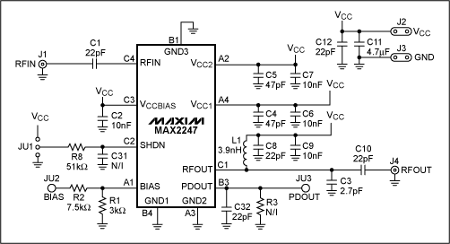
Figure 1. Schematic diagram of MAX2247, optimized for 802.11g 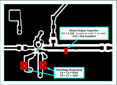
Figure 2. Optimal location of VCC1 and VCC2 bypass capacitors and output matching capacitors 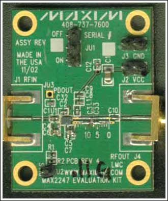
Figure 3. Close-up photo showing the location of the component
3000A Fuse for the Protection,The Protection of Semiconductor Device,Fuse for the Protection
YANGZHOU POSITIONING TECH CO., LTD. , https://www.yzpst.com