
In the field of chip research and development, FPGA verification plays a crucial role. One of the key challenges is how to effectively utilize FPGA resources and assign pins in an optimal way. A common approach is to rely on automated tools during synthesis by applying timing constraints. However, this method may not always be practical due to time constraints in the development cycle. As a result, RTL verification and board design must be closely aligned. The verification board needs to be designed before the design code is finalized, meaning that pin assignments often have to be done manually rather than relying on tools. This makes the process more complex, as it requires careful consideration of multiple factors.
**Consider the following aspects:**
1. **Signal flow within the FPGA logic**
FPGAs used for IC verification typically have large logic capacity and numerous I/O pins. When assigning pins, it's important to consider the PCB layout and signal routing. Poor pin assignment can lead to many crossed signals, making wiring difficult and potentially causing timing issues due to excessive external delay. Before assigning pins, it's essential to understand the environment in which the FPGA operates. Signals should be assigned to the nearest available pin connected to external devices, following the principle of shortest path connections within each BANK.
2. **Understanding internal BANK allocation**
Modern FPGAs are divided into multiple BANKs, each with different I/O capabilities. For example, Altera and Xilinx FPGAs have distinct BANK structures. Understanding these allocations is critical. Here’s an example of the BANK structure in Altera’s Stratix II series:
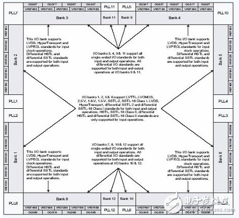
This diagram shows the distribution of BANKs and the supported I/O standards in each. By aligning this with the signal flow from Figure 1, you can determine the best placement for signals, ensuring they are assigned to the closest and most suitable BANK.
3. **I/O standards per BANK**
Each BANK supports specific I/O standards. When assigning pins, it's important to group signals that require the same standard into the same BANK. While some exceptions exist, most BANKs do not support multiple I/O standards simultaneously. Always refer to the device manual to confirm compatibility and avoid conflicts.
4. **Special signal pin assignment**
Special signals such as clock and reset lines require careful handling. Clocks should be assigned to global clock pins to minimize delay and maximize drive strength. Similarly, reset signals benefit from strong driving capability and synchronization, so they are usually connected to the same global clock pin. When dealing with multiple clocks, especially differential ones, ensure that P and N terminals are not assigned to different signals at the same time. For instance, in Xilinx FPGAs, paired clocks cannot be routed to the same area simultaneously. It's better to use only one of the pair to avoid conflicts.
5. **Signal integrity considerations**
Bus signals often involve multiple lines switching simultaneously, which can cause signal integrity issues like crosstalk or noise. To mitigate this, it’s advisable to separate high-toggle buses across different pins or BANKs. This helps reduce interference and improves overall system performance.
By carefully considering these factors, engineers can achieve more reliable and efficient FPGA designs, ensuring both functional correctness and physical feasibility.
Non Electronic Passive Stylus Pen,Universal Passive Stylus Pen,Passive Touch Stylus Pen,Simple Passive Stylus Pen
Shenzhen Ruidian Technology CO., Ltd , https://www.wisonen.com