
introduction
This article refers to the address: http://
There are two mainstream implementation solutions for video capture: one is based on ASIC, which generally uses dedicated video processing chips from companies such as STMicroelectronics and AMD; the other is based on DSP, which mainly uses DSP signal processors from companies such as TI and ADI.
As a secondary processor, they can capture and compress video signals under the control of the main CPU. With the development of FPGA, video acquisition through SOPC technology has become a solution that is easy to develop and flexible in design. This is mainly due to the development of IP multiplexing technology. Building complex embedded systems on an FPGA can take advantage of existing functional modules and their drivers. The solution has greater integration and flexibility, and will therefore become a major trend in the development of electronic design.
This article describes the design of a universal video capture system using Xilinx's Spartan-3 FPGA. The system is externally connected to the analog PAL/NTAL camera, which can capture video signals in real time and compress and encode them in MPEG-4 format. The code stream can be transmitted to the PC through the USB interface or transmitted through the Ethernet interface. This system selects the XC3S200 chip of Spartan-3 FPGA series. The chip has 4320 logic cells (LC), 216Kbit block RAM, 4 digital delay phase-locked loops (DDL), 173 user I/Os, and high logic density. , I / O and low cost. This design mainly involves board-level hardware design, FPGA-level hardware system design and system software design.
1 board level hardware design
With the support of the power supply and configuration circuitry, the FPGA can form a minimal system for embedded systems and can implement all the functions on-chip. In this minimization system, the functional module circuits such as the external storage module, the video acquisition module, the USB interface module, and the Ethernet interface module can be extended according to the application requirements of the design, thereby forming a circuit board level hardware platform. The structure of the board-level hardware platform is shown in Figure 1.
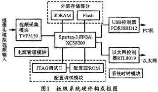
1.1 Minimize the system
The FPGA is a device based on an SRAM memory structure. Configuration data can be loaded from external configuration memory into internal SRAM each time it is powered up, allowing it to build a logical structure for logic functions. The configuration debug module mainly includes configuration memory, configuration mode jumper switch and JTAG debug port. The JTAG debug port is a communication interface between the PC and the FPGA in the system development phase, and can be used to download FPGA configuration data from the PC, and is used in the program debugging phase. Online interface. This design uses Xilinx Platform Flash series configuration memory XCF02S, and uses a 14-pin JTAG interface. The mode jumper switch determines whether the FPGA is configured by JTAG or by configuration memory. The system clock module provides a 50 MHz high frequency clock signal to the XC3S200, which uses a highly stable quartz crystal oscillator discrete component. The power management module uses a DC/DC converter to provide the various voltage and current required for each component of the system. The above part is connected to the FPGA chip to form a minimum system for the embedded system to work.
1.2 External Storage Expansion
Due to the limited on-chip storage capacity of the XC3S200 and loss of power, it is necessary to configure a large-capacity external storage. This design extends 4MByte flash and 32MByte SDRAM (including one AMD AM29LV320DT90EC Flash and two HYNIX HY57V281620HCT-PI SDRAM). Flash is used in the system to store program code, constant tables, and some user data that needs to be saved after the system is powered off. The SDRAM power-down data is lost, but its access speed is much higher than Flash and readable and writable, so it is used as the running space, temporary data and stack area of ​​the program in the system.
1.3 Video Acquisition Module
The TVP5150 is an ultra-low-power, high-performance mixed-signal video decoder chip from TI that automatically recognizes NTSC/PAL/SECAM analog signals and converts them into digital signals in YCbCr4:2:2 format. It is then output in the ITU-RBT.656 format with 8-bit embedded sync signals. The TVP5150 features low price, small size and easy operation. The operation of the FPGA on the TVP5150 chip is realized through the I2C bus, and the data transmission connection method adopts the simplest ITU-RBT.656 mode.
1.4 USB interface module
The USB interface module uses PHILIPS' high-performance USB interface chip PDIUSBD12. The chip is fully compliant with the USB 1.1 specification, supports DMA transfers, and communicates with the FPGA via a high-speed 8-bit parallel interface with a maximum parallel interface rate of 2 MB/s.
1.5 Ethernet interface module
The module uses the highly integrated Ethernet controller RTL8019AS from Realtek. The RTL8019AS supports the IEEE802.3 standard and an 8-bit or 16-bit data bus. Its built-in 16KB SRAM can be used for transceiver buffering. In full-duplex mode, its transmission and reception can reach 10Mbps at the same time. The RTL8019AS supports 10Base5, 10Base2, and 10BaseT and automatically detects connected media. This design uses the RTL8019AS jumper interface mode and connects to the FPGA via a 16-bit data bus.
2 chip level hardware system design
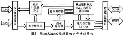
The foundation for building an embedded system on Spartan-3 is the MicroBlaze IP core. This is a 32-bit microprocessor implemented in the FPGA with a hardware description language, using the RISC instruction set and the Harvard architecture. It can be customized for different peripheral and memory configurations, and the processor system architecture can be tailored to the application. This configuration takes up approximately 500 Slices on the Spartan-3 family of chips. The IP core has 32 32-bit general purpose registers and 2 special registers. Its 32-bit wide instruction system supports three operands and two addressing modes, while its separate 32-bit instruction and data bus is fully compatible with IBM's OPB bus. Through the LMB bus in the module, its 32-bit instructions and data can be directly connected to the on-chip block memory. In addition, the IP core also features high-speed instruction and data cache (Cache), three-stage pipeline structure, 32-bit address bus, hardware debug logic, eight inputs and eight output fast link (FSL) interfaces. The internal functional structure of the MicroBlaze soft processor is shown in Figure 2.
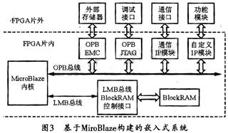
When designing an embedded system on an FPGA, you can develop an on-chip peripheral IP core on the lowest layer hardware resources, or use the developed IP core to build the hardware part of the embedded system, and then develop the IP core device driver and application interface (API). ) and application layer (algorithm). The local memory bus (LMB) and the on-chip peripheral bus (OPB) are connected to the on-chip peripheral IP core via a standard bus interface, and the MicroBlaze processor can be connected to various peripheral IP cores and on-chip BlockRAM. The IP core provided by the development tool has corresponding device driver and application interface, and the user only needs to use the corresponding function library to write his own application software and algorithm program. For the user-developed IP core, you need to write the corresponding driver and interface functions. The basic embedded system built using the MicroBlaze processor is shown in Figure 3.
Implementing an embedded system on an FPGA is mainly to build an on-chip MicroBlaze processor, and add on-chip peripherals to the processor to implement hardware module functions. At the same time, the on-chip peripherals should be connected to the external pins of the chip. While developing on-chip peripherals, you should develop the underlying drivers for peripheral functions and then implement the system applications on the MicroBlaze processor. This is a process of collaborative development of software and hardware. The system development based on the MicroBlaze processor can use the EDK (Embedded Development Kit) provided by Xilinx. The EDK provides an integrated development environment XPS (Xilinx Platform Studio) that integrates tools such as hardware platform generators, software platform generators, simulation model generators, software compilers, and software debuggers. In this environment, various tools can be called to complete the whole process of software and hardware collaborative development. EDK offers a variety of functional IP cores related to MicroBlaze processors, including OPB 10/100M Ethernet controllers, PLB/OPB SDRAM controllers, UART interrupt controllers, timers and other peripheral interfaces. Use the System Hardware Builder in the EDK to configure the MicroBlaze processor, and use the ImportPeripheral Wizard to call the existing IP core to generate the on-chip device and the processor. The bus is connected.
The main function modules of the system include video interface module, ring buffer, code stream two-stage FIFO buffer, MPEG-4 encoder, flash controller, SDRAM controller, 10/100M Ethernet control module, USB control module. Wait. The video interface module is the interface between the MicroBlaze processor and the TVP5150. The MicroBlaze processor's control driver for the TVP5150 can be ported from the TVP5150 driver template, which can be used to configure the TVP5150 acquisition mode and store the captured video signal in a 4:2:0YUV format in a ring buffer. The ring buffer is part of the on-chip SRAM memory space connected to the MicroBlaze processor bus, where the data queue's head and tail pointers are maintained by the MicroBlaze processor program. Using the FIFO template provided by the development tool, parameters such as depth, bit width, read/write clock, full flag, etc. can be set, and two FIFOs are connected to form a two-stage FIFO, and then the entrance is matched with the MPEG-4 encoder. The output is connected. The first stage of the FIFO is connected to the MicroBlaze processor bus to support DMA reading. The MPEG-4 encoder is a Xilinx-licensed MPEG-4 Simple Profile encoder IP core that accepts uncompressed 4:2:0YUV format video signals in a ring buffer and can generate MPEG-4 Simple Profile compressed streams. . The MPEG-4 encoder is connected to the MicroBlaze processor bus and two levels of FIFO inputs to provide its drivers for EDK. The implementation software for the Flash controller, SDRAM controller, and 10/100M Ethernet controller is provided in the EDK. The connection to the processor bus is also automatically set in the wizard tool, and the driver is included. Because the off-chip uses a highly integrated USB controller, and the on-chip USB control module is only the direct connection between the MicroBlaze processor bus and the pins, the driver is only a reference to the PDIUSBD12 general driver on the EDK software platform.
The connection between the on-chip peripherals of this system and the MircoBlaze processor is shown in Figure 4, where the arrows indicate the flow of video data. 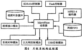
3 system software design
The control driver for the TVP5150 and PDIUSBD12 of the MicroBlaze processor in the system can be ported on the EDK software platform according to its universal driver. The IP core provided by Xilinx can be used to build an FPGA on-chip hardware platform, and at the same time, the underlying hardware driver can be supported, and then the system application can be developed on the basis of this.
After the external analog video signal is converted into a digital video signal by the TVP5150, it can enter the FPGA and be directly arranged to the end of the internal ring buffer data queue through the video interface module.
When the MircoBlaze processor receives an interrupt available to the MPEG-4 encoder, the system will detect if the ring buffer is empty. When not empty, the header data of the data queue can be taken out to the MPEG-4 encoder, and the encoder code is started.
After the video signal is encoded into the video original code stream by the encoder, it can enter the internal secondary FIFO buffer of the FPGA. A data output interrupt request is issued to the MircoBlaze processor when the FIFO is first level.
After responding to the interrupt from the FIFO, the MircoBlaze processor can take out the FIFO first level data and output it as a USB or Ethernet interface, and then clear the FIFO first level.
According to the above work process, the application of the MircoBlaze processor includes the following parts:
(1) System reset initialization
That is to prohibit external interrupts, initialize each driver, clear the ring buffer and two-stage FIFO, detect the USB interface, Ethernet interface connection to determine the way to output, then start the control of TVP5150 and data acquisition, and finally enable external interrupt .
(2) Encoder available interrupt service
The encoder completes one frame of data encoding to issue an interrupt to the MircoBlaze processor, and then the MircoBlaze processor controls the encoder to extract data from the ring buffer and waits for a certain amount of time when the ring buffer is exhausted;
(3) code stream can output interrupt service
When the code output of the two-stage FIFO first level is ready to be output, an interrupt can be sent to the MircoBlaze processor, and then under the control of the MircoBlaze processor, the code stream is delivered to the USB or Ethernet output interface API and output by the underlying driver. Finally, empty the FIFO first.
Figure 5 shows its application flow chart. 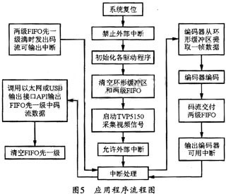
4 Conclusion
This design introduces the implementation of a universal video acquisition system based on Spartan-3 FPGA. The design of this system relies on dedicated design software and IP modules. Due to the adoption of SOPC technology, the system can be reduced, scalable, and upgradeable, and the high degree of multiplexing of multi-level IP modules makes the system have the advantages of short design cycle, low risk investment and low design cost.
Stranded Loose Tube Optical Fiber Cable
Optical Ground Wire,Stranded Loose Tube Optical Fiber Cable,Stranded Loose Tube Armored Cable,Loose Tube Fiber Optic Cable
Shandong Qingguo Optical Fiber Co., Ltd. , http://www.qgfiber.com