
The Σ-Δ ADC plays a vital role in modern signal acquisition and processing systems. This article aims to provide readers with a clear understanding of the fundamental principles behind the Σ-Δ ADC architecture. It explores key trade-offs involving noise, bandwidth, settling time, and other critical parameters that influence ADC subsystem design.
A typical Σ-Δ ADC consists of two main components: a sigma-delta modulator and a digital signal processing module, often implemented as a digital filter. A simplified block diagram and key concepts of the Σ-Δ ADC are illustrated in Figure 1.
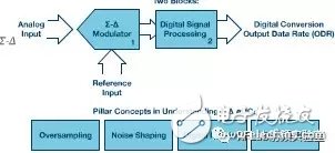
**Figure 1. Key concepts of Σ-Δ ADC**
The sigma-delta modulator is an oversampling architecture, so it’s important to first understand Nyquist sampling theory and oversampling techniques. Figure 2 compares three different ADC operation schemes: standard Nyquist mode, oversampling, and sigma-delta modulation.
In Figure 2a, the quantization noise is evenly distributed across the Nyquist bandwidth (FS/2), determined by the ADC's LSB size. In Figure 2b, when the system operates at an oversampling rate (K × FS), the noise spreads over a wider bandwidth (K × FS/2). A low-pass digital filter then removes the noise outside the desired frequency range.
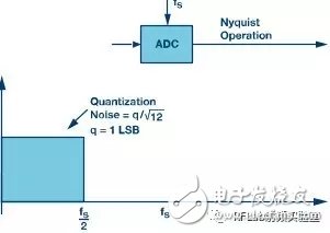
**Figure 2a. Nyquist scheme. Sampling rate is FS, Nyquist bandwidth is FS /2**
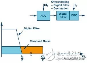
**Figure 2b. Oversampling scheme. Sampling rate is K × FS**
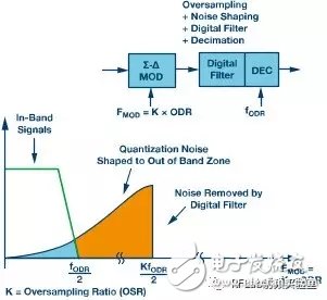
**Figure 2c. Σ-Δ ADC scheme. Oversampling and noise shaping, sampling rate is FMOD = K × FODR**
One of the key advantages of the sigma-delta modulator is noise shaping. As shown in Figure 2c, the quantization noise is pushed to higher frequencies, where it can be easily filtered out. The noise floor of a Σ-Δ ADC is primarily determined by thermal noise rather than quantization noise.
**Sampling, Modulation, Filtering**
The Σ-Δ ADC uses either an internal or external sample clock. The main clock (MCLK) is usually divided before being used by the modulator. Understanding the relationship between the MCLK and the modulator frequency is crucial when interpreting ADC data sheets. The modulator samples at a rate FMOD, and the digital filter processes this output to generate the final data at the output data rate (ODR). Figure 3 illustrates this process.
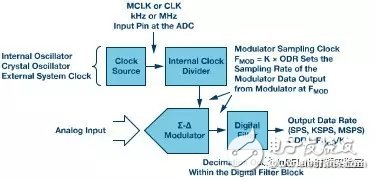
**Figure 3. Σ-Δ ADC flow: from modulator output to digital filtering**
**Output Sampling**
The sigma-delta modulator functions as a closed-loop system with a low-resolution ADC and DAC. The output is typically a single-bit signal that represents either a high or low state. When the input changes, the modulator adjusts its output accordingly. For example, a sine wave input results in a varying density of +1 and –1 states in the output. When the input reaches full scale, the output remains mostly in one state. The output switching rate reflects the input's rate of change, effectively encoding the analog signal into a digital form.
A linear model of a 1-bit modulator (Mod 1) shows how the system behaves as a feedback control loop. The quantization noise is the difference between the input and the output of the quantizer. This noise is shaped by the loop filter, which acts as a low-pass filter for the signal and a high-pass filter for the noise.
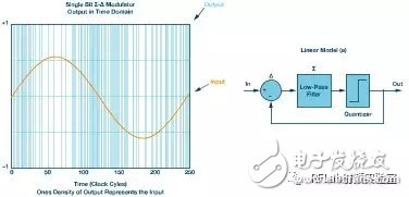
**Figure 4. Density of the Σ-Δ output 1 code value of the input sine wave. Linear model of a 1st order Σ-Δ modulator loop (a)**
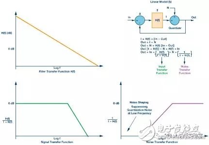
**Figure 5. Linear model of the Mod 1 Σ-Δ loop (b), including equations, filters, signals, and noise transfer function diagrams**
By solving the equations in Figure 5, we can derive the signal and noise transfer functions. The signal transfer function acts as a low-pass filter, while the noise transfer function shapes the quantization noise into a high-pass characteristic. For a first-order modulator (Mod 1), the noise increases at 20 dB/decade.
To improve resolution, higher-order modulators are often used. Cascading loop filters increases the roll-off of the noise transfer function, resulting in a steeper noise shaping slope—typically 40 dB/decade for a second-order modulator (Mod 2). This allows for better noise suppression at lower frequencies.
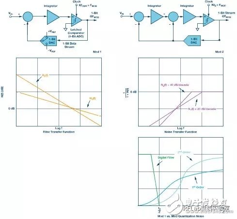
**Figure 6. Mod 1 and Mod 2 block diagram configuration and comparison of filter and noise transfer functions**
There are many variations of sigma-delta modulators. One popular approach is the multi-level noise shaping (MASH) architecture, which avoids the stability issues of high-order single-bit loops. This architecture enables the design of stable, high-performance ADCs using combinations of low-order loops.
Single Phase Vfd,220V Frequency Inverter,Ac Frequency Inverter,High Frequency Inverte
WuXi Spread Electrical Co.,LTD , https://www.vfdspread.com