The Σ-Δ ADC is a crucial component in the toolset of modern signal acquisition and processing system designers. This article aims to provide readers with a foundational understanding of the Σ-Δ ADC architecture. It explores key trade-offs between noise, bandwidth, settling time, and other essential parameters involved in ADC subsystem design.
Typically, a Σ-Δ ADC consists of two main components: a sigma-delta modulator and a digital signal processing module, often a digital filter. A simplified block diagram and core concepts of the Σ-Δ ADC are illustrated in Figure 1.
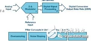
**Figure 1. Key concepts of Σ-Δ ADC**
The sigma-delta modulator operates under an oversampling architecture, so we begin by reviewing Nyquist sampling theory and oversampling ADC operation.
Figure 2 compares three different ADC approaches: the standard Nyquist mode, the oversampling scheme, and the sigma-delta modulation (also an oversampling technique).
In Figure 2a, the quantization noise is spread across the Nyquist band (FS/2), determined by the ADC's least significant bit (LSB). In Figure 2b, when the ADC operates in an oversampling mode, the sampling rate increases by a factor of K, spreading the quantization noise over a wider bandwidth. A low-pass digital filter then removes the noise outside the desired frequency range.
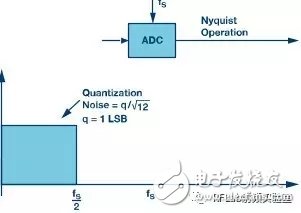
**Figure 2a. Nyquist scheme. Sampling rate is FS, Nyquist bandwidth is FS /2**
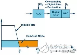
**Figure 2b. Oversampling scheme. The sampling rate is K × FS**
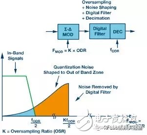
**Figure 2c. Σ-Δ ADC scheme. Oversampling and noise shaping, sampling rate is FMOD = K × FODR**
One unique feature of the sigma-delta modulator is noise shaping, as shown in Figure 2c. The quantization noise is shifted to higher frequencies, where it can be easily filtered out by a low-pass digital filter. As a result, the noise floor of a Σ-Δ ADC is primarily determined by thermal noise rather than quantization noise.
**Sampling, Modulation, Filtering**
The Σ-Δ ADC uses either an internal or external sample clock. The main clock (MCLK) is usually divided before being used by the modulator. Pay attention to this detail when reviewing ADC datasheets, as it affects the modulator’s operating frequency. The clock sent to the modulator defines the sampling frequency (FMOD). The modulator outputs data at that rate, which is then processed by a digital filter—often a low-pass filter with decimation—to produce the final output data rate (ODR). Figure 3 illustrates this process.
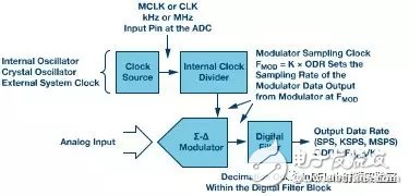
**Figure 3. Σ-Δ ADC flow: from modulator output to digital filtering**
**Output Sampling**
The sigma-delta modulator functions as a negative feedback system, similar to a closed-loop amplifier. It includes a low-resolution ADC and DAC, along with a loop filter. The output is typically a one-bit signal, representing either a high or low state. The ADC’s analog system implements this structure, with the quantizer performing the actual sampling. If the loop remains stable, the output provides a rough representation of the input. The digital filter then refines this coarse output into a precise digital conversion of the analog input.
Figure 4 shows the density of the modulator output in response to a sine wave input. The rate at which the modulator switches between high and low states depends on the input’s rate of change. When the sine wave reaches full scale, the switching rate decreases, and the output becomes dominated by a single state. When the input changes rapidly, the modulator produces a higher density of transitions. This behavior ensures that the analog input is accurately represented by the modulator’s output slew rate.
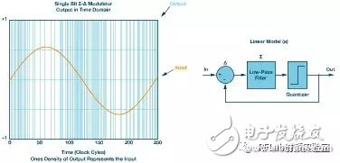
**Figure 4. Density of the Σ-Δ output 1 code value of the input sine wave. Linear model of a 1st order Σ-Δ modulator loop (a)**
If we model the 1-bit modulator (Mod 1) linearly, the system behaves like a control system with negative feedback. The quantization noise is the difference between the input and the quantized output. This noise is passed through a low-pass filter, as shown in Figure 5b, where it is represented by N.
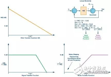
**Figure 5. Linear model of the Mod 1 Σ-Δ loop (b), including equations, filters, signals, and noise transfer function diagrams**
By solving the equations in Figure 5, we can derive the signal and noise transfer functions. The signal transfer function acts as a low-pass filter with a gain of 1 within the target bandwidth. The noise transfer function behaves as a high-pass filter, providing noise shaping and suppressing quantization noise near DC. For a first-order modulator (Mod 1), the noise increases at a rate of approximately 20 dB/decade.
To enhance system resolution, a common approach is to cascade multiple loop filters, increasing the loop order. This results in a steeper roll-off and improved noise shaping. A second-order modulator (Mod 2) exhibits a noise increase of about 40 dB/decade. Figure 6 compares Mod 1 and Mod 2 configurations.
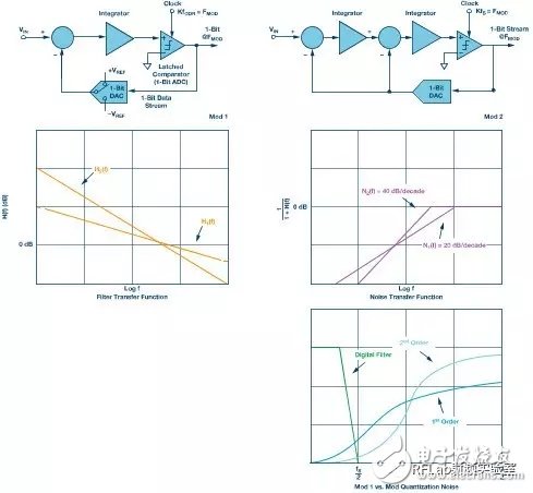
**Figure 6. Mod 1 and Mod 2 block diagram configuration and comparison of filter and noise transfer functions**
The Σ-Δ modulator has many variations, but one notable architecture is the multi-level noise shaping modulator (MASH). This design avoids stability issues in high-order 1-bit loops by using multiple stages with inherent stability. MASH allows for the implementation of stable, high-order Σ-Δ modulators using combinations of lower-order loops.
Single Phase VFD
A single-phase VFD, also known as a variable frequency drive, is a specialized electronic device used for precise control and regulation of single-phase motors. Unlike three-phase motors that are commonly used in industrial applications, single-phase motors are predominantly found in residential and small-scale applications.
The primary function of a single-phase VFD is to control the frequency and voltage supplied to the single-phase motor, thereby enabling accurate regulation of motor speed. By adjusting the frequency and voltage output, the VFD allows for smooth and precise control over the motor's rotational speed. This feature is particularly useful in applications where speed control is required, such as in residential HVAC systems, small-scale machinery, and household appliances.
Energy efficiency is a significant advantage offered by single-phase VFDs. By adjusting the motor speed to match the load requirements, the VFD reduces energy wastage and improves overall energy efficiency. When the motor operates at a lower speed during periods of low demand, energy consumption is significantly reduced, resulting in energy savings and lower operating costs.
Motor protection is another important aspect addressed by single-phase VFDs. They incorporate various protective features, including overload protection, short circuit detection, and thermal protection, which help safeguard the motor against damage due to excessive current, voltage fluctuations, or overheating. This ensures reliable motor operation, prolongs the motor's lifespan, and reduces the risk of unexpected failures.
Harmonic filtering is also a critical consideration in single-phase VFD applications. When single-phase VFDs operate, they can introduce harmonics into the power supply, which may cause issues such as voltage distortions and interference with other electrical equipment. To mitigate these problems, single-phase VFDs often incorporate harmonic filtering techniques to suppress harmonics and ensure a clean and stable power supply, maintaining power quality and preventing damage to connected equipment.
Control algorithms play a significant role in single-phase VFD operation. These algorithms allow for precise control and adjustment of motor speed, ensuring smooth acceleration, deceleration, and accurate speed regulation. Advanced control algorithms enable efficient motor operation and enhance overall system performance.
In summary, single-phase VFDs provide precise control and regulation of single-phase motors in residential and small-scale applications. With their energy efficiency, motor protection features, harmonic filtering capabilities, and advanced control algorithms, single-phase VFDs enhance motor performance, reduce energy consumption, and ensure reliable operation in various residential and small-scale applications.
Single Phase Vfd,220V Frequency Inverter,Ac Frequency Inverter,High Frequency Inverte
WuXi Spread Electrical Co.,LTD , https://www.vfdspread.com
