
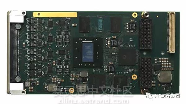
TEWS Technology's TXMC638 is a high-performance XMC card featuring 24 ADC channels, 16-bit resolution, and a sampling rate of 5 million samples per second. It integrates the Linear Technology LTC2323-16 analog-to-digital converter, which operates at 5Msps using a successive approximation register architecture. This card is designed for use in programmable data acquisition systems and includes a Xilinx Kintex-7 FPGA (available in K160T, K325T, or K410T variants) along with a 1GB 32-bit wide DDR3 SDRAM chip for on-board memory. The TXMC638 also offers three 100-ohm AC-coupled differential input terminals with a wide voltage range, all connected through a 98-pin Samtec ERF8-049 connector.
The FPGA on the TXMC638 comes preloaded with a reference design, making it easy to get started. In addition to programming the FPGA via Xilinx’s USB programmer, users can also load designs through the on-board configuration controller (BCC). For system-level programming, the FPGA can be configured via serial SPI flash, while real-time debugging and data reading are supported through the JTAG port. For PCIe compatibility, the Xilinx Tandem configuration method is available, with "Tandem PROM" being the recommended approach. Below is the block diagram of the XMC capture card:
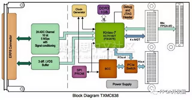
The Kintex-7 FPGA used on this board is built on a 28nm process, significantly reducing power consumption compared to earlier generations while doubling the performance-to-cost ratio. The Kintex-7 family provides high-density logic (up to 478K logic cells), high-speed serial connectivity (up to 1.6Gb/s), DDR memory support, high-speed transceivers (up to 12.5Gb/s), DSP capabilities, a PCI Express interface, and 16-channel dual 12-bit DACs.
The differential ADC inputs on the card handle ±2.5V signals and output a ±5V differential voltage range. Additionally, the XMC P14 connector provides 64 digital I/O pins that support 64 single-ended LVCMOS 24 or 32 differential LVDS25 interfaces, while the P16 connector includes four 12.5Gbps GTX transceiver pins.
According to the TEWS datasheet, developers can create custom data acquisition and control applications for the TXMC638 using the Xilinx Vivado Design Suite. Launched in 2012, Vivado is an integrated design environment that combines advanced tools from the system level down to the IC level. Based on a shared scalable data model and a common debugging environment, Vivado supports not only programmable logic design but also full system integration. As more functions are consolidated onto fewer chips, Vivado continues to evolve as a powerful tool for modern FPGA-based systems.
oxides, nitrides, silicides, borides, and carbides
Yixing Guangming Special Ceramics Co.,Ltd , https://www.yxgmtc.com