
At present, high frequency and high efficiency DCDC converters are increasingly used in automotive electronic systems.
The high switching frequency allows the use of smaller power inductors and output filter capacitors, resulting in a reduced overall system size, increased system compactness and reduced system cost; high operating efficiency can increase the use of automotive batteries Time, reduce the power loss of the system, thereby reducing the heat generated by the system, optimizing the thermal design of the system, and further improving the reliability of the system.
However, the high switching frequency will reduce the efficiency of the system, so there must be some trade-off between switching frequency and operating efficiency. This article focuses on the DCDC step-down BUCK converter used in automotive electronic systems, to explore some of the design techniques and considerations including the above problems, and these problems are often the details that are easily overlooked in the current design of the project.
1 Actual minimum and maximum input operating voltage
1.1 Switching frequency
The switching frequency must be traded off between efficiency, component size, minimum input-to-output voltage difference, and maximum input voltage. The high switching frequency reduces the value of the inductor and capacitor, so smaller inductors and capacitors can be used and the cost can be reduced. However, high switching frequencies reduce efficiency and reduce the actual maximum operating input voltage, as well as requiring higher input-to-output voltage differences.
The highest switching frequency can be calculated by: 
Where: f S ( MAX ) is the maximum switching frequency, t ON ( MIN ) is the minimum on-time required by the switch, V D is the forward voltage drop of the freewheeling diode, V OUT is the output voltage, V IN is The input voltage for normal operation, V DS ( ON ) is the conduction voltage drop of the switching transistor.
The above equation shows that when t ON ( MIN ) is constant, a low duty cycle requires a lower switching frequency to ensure safe operation of the system. Similarly, a low switching frequency allows for lower input and output voltage differences.
The main reason why the input voltage depends on the switching frequency is that the PWM controller has a minimum turn-on t ON ( MIN ) and a minimum turn-off time t OFF ( MIN ) . If the value is 150ns, that is, the on-time must be at least 150ns when the switch is turned on, and less than 150ns may cause the MOSFET to not turn on normally. Similarly, the switch should be turned off for at least 150ns when the switch is turned off. Below 150ns may cause the MOSFET to fail to turn off properly. This means that the minimum duty cycle and maximum duty cycle are: 
The above equation shows that the duty cycle range increases as the switching frequency decreases. The optimized switching frequency must ensure that the system has a sufficient input operating voltage range while making the inductance and capacitance as small as possible.
1.2 Actual maximum input operating voltage
Usually the input voltage of the chip has a certain rated operating voltage range. In addition to the rated operating voltage limit, the actual input operating voltage is limited by other conditions. The minimum actual input operating voltage is usually determined by the maximum duty cycle. The duty cycle of the BUCK converter is: 
At the highest input voltage, the duty cycle is minimal. The maximum actual input operating voltage is determined by the minimum duty cycle of the PWM controller: 
If the output is under starting or short-circuit operating conditions, the input voltage must be lower than the following calculation: 
It can be seen that the low switching frequency can be operated safely at higher input voltages. The shortest on-time t ON ( MIN ) is the minimum duration each controller can turn on the high-side MOSFET. It is determined by the internal timing delay and the amount of gate charge required to turn on the high-side MOSFET. Low duty cycle applications can approach this minimum on-time limit and care should be taken to ensure that: 
If the output voltage is in the regulated state, the system is not a start and short circuit condition. The input voltage is greater than the allowable actual maximum input operating voltage, and the system can still operate regardless of the operating frequency. In this case, the duty cycle drops below the level at which the minimum on-time can be adjusted, and the controller will begin to enter the skip mode of operation, ie some pulses will be skipped to maintain the output voltage regulation, at which time the output voltage And the current ripple is larger than the voltage and current ripple output during normal operation.
Generally, when the peak detection voltage drops, the minimum on-time of each controller will gradually increase. For example, under light load conditions, the minimum on-time will gradually increase, in a forced continuous operation application with low ripple current. It is especially important that in this case the duty cycle drops below the minimum on-time limit and a significant jump pulse occurs, with a significant increase in current and voltage ripple. In addition, the saturation current of the inductor is usually more than 1.3 times of the output current. For some harsh operating conditions such as start-up and output short-circuit and high input voltage, the saturation current of the inductor must be taken to a larger value to ensure safe operation of the system.
Usually the switching frequency is fixed, but some synchronous BUCK controllers that use an external resistor to set the switching frequency can add a Zener Z1 and a current-limiting current R1 to reduce the switching frequency when the input voltage increases, thus expanding the range of the input voltage, such as Figure 1 shows. 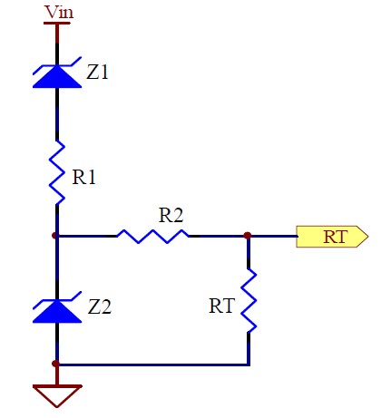
Figure 1: Down-conversion operating circuit at high input voltage
The problem caused by this circuit is that at high input voltages, the output current and voltage ripple increase due to the frequency reduction and the inductance value. The frequency varies over a wide range, the inductance cannot be optimized, and the compensation of the loop cannot be optimized. The range of frequency variations is limited by increasing the Zener Z2 and current-limiting current R2 to set the minimum operating frequency of the system.
1.3 Actual minimum input operating voltage
The duty cycle is maximized when the input voltage is lowest. With a synchronous BUCK controller, the minimum actual input operating voltage is determined by the maximum duty cycle of the PWM controller: 
The relationship between the minimum operating voltage and the minimum off time t OFF ( MIN ) is: 
It can be seen from the above formula: When t OFF ( MIN ) is fixed, the high switching frequency will increase the actual minimum input operating voltage. For lower input operating voltages, a lower switching frequency can be used. In some synchronous BUCK controllers, when the differential pressure between the input and output drops to a certain value, the system enters a full-conduction or LDO control with a 100% duty cycle.
2 transient maximum peak input voltage
As battery-powered devices increasingly enter the field of mobile applications, people use the car's cigarette lighter to turn on the power so that the battery pack can store and even recharge the car while it is running. Before turning it on, note that the main power cable inside the car generates some potential transients, including load dump and voltage voltage multiplication, when connected to a very poor power source. Load dump is the result of loose battery cables. When the cable connection is interrupted, the magnetic field in the alternator produces a positive spike of up to 60V, which decays in a few hundred milliseconds. Battery voltage multiplication is the result of a colder car that is faster than 12V when the 24V jump start is achieved.
Figure 2 is the easiest and straightforward way to protect the DCDC converter from damage from the car's power cord.
The transient suppressor clamps the input voltage during a load dump. Note: The transient suppressor should not be turned on during double battery voltage operation, but the input voltage must still be clamped below the converter's breakdown voltage. 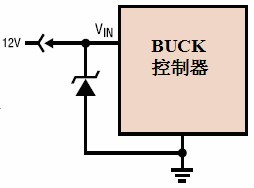
Figure 2: Input TVS protection circuit
Ceramic capacitors are small in size, low in impedance, and have a wide operating temperature range, making them ideal for use in the input bypass capacitors of BUCK converters in automotive electronics. However, when the input power of the BUCK converter is inserted into the working power supply, that is, hot insertion, such as a cigarette lighter of a car, these ceramic capacitors have problems in application: the low-loss ceramic capacitor and the stray inductance of the connecting wire are low-impedance. The power supply forms an underdamped resonant ring that oscillates, creating a spike in the input supply voltage at the input of the BUCK converter, which exceeds the allowable voltage rating at the input of the BUCK converter, damaging the device. Under this operating condition, the input absorption network must be designed to prevent overshoot spikes in the input voltage. The waveform below shows the waveform of a BUCK converter connected to a 24V supply from a 6-foot twisted pair. Figure 3 shows the response of the input with only a 4.7uF ceramic capacitor. The peak value of the input voltage is 50V, and the peak value of the input current is 26A. 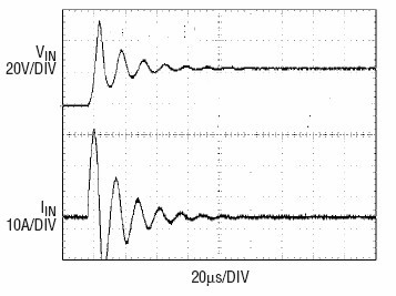
Figure 3: Input response with only 4.7uF ceramic capacitor input
The use of damped oscillations can reduce the peak voltage. There are two ways to form a damped oscillation: 1 input ceramic capacitor adds a series resistor; 2 uses electrolytic capacitor. Aluminum electrolytic capacitors have a high ESR, which can form a damping and reduce the overshoot of the oscillation; its capacitance can filter out the low frequency ripple, and the efficiency of the system is slightly improved. It's just a relatively large volume. Figure 4 shows the response of a 22uF electrolytic capacitor and a 4.7uF ceramic capacitor in parallel with the input. The ceramic capacitor filters out high frequency ripple. The peak value of the input voltage is significantly reduced. 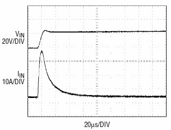
Figure 4: Response of a 4.7uF ceramic capacitor with an input of 22uF electrolytic capacitor in parallel
Adding a 0.7 ohm series resistor to the input also reduces voltage overshoot while reducing the peak current. A 0.1uF small ceramic capacitor filters out high frequency ripple. As shown in Figure 5 (a).
Compared with the electrolytic capacitor method, this method is small in size and low in cost, and has little influence on the efficiency of the system at a high input voltage. However, when the input voltage is relatively low, the efficiency of the system is slightly reduced. 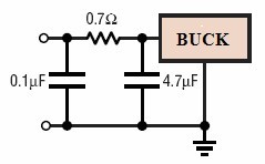
(a) 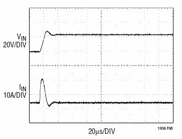
(b)
Figure 5: Response of input plus series resistor
3 thermal design
The power MOSFET selection criteria include on-resistance R DS ( ON ) , Miller capacitance C MILLER , input voltage and maximum voltage and maximum output current. The C MILLER can be approximated by the gate charge curve given by the MOSFET's product data. C MILLER is equal to the increase of gate charge along the horizontal axis, and the curve is roughly divided by the specified variation level of VDS, and then the result is multiplied by the VDS ratio specified by the VDS applied to the application and the charging curve of the gate. The high-side and low-side MOSFET duty cycles for operating CCM are given by:
Main switch duty cycle: D Â = V OUT /VIN.
Synchronous switch duty cycle: V IN -V OUT /V IN .
The power dissipation of the MOSFET under the maximum output current condition is given by: 
Where: δ is the temperature coefficient of R DS ( ON ) , R DR is about 4 ohms, which is the effective driving resistance under the MOSFET Miller threshold voltage, and V THMIN is the typical threshold voltage of the typical MOSFET.
Both MOSFETs have I 2 R losses, while the high-end N-channel equation contains an additional term for calculating conversion losses, which is greatest at high input voltage conditions. <20V when using generally large MOSFET can improve the efficiency of a large current, and when V IN> 20V when V IN during rapid conversion loss increases. At this time, using a higher R DS ( ON ) device and a lower C MILLER can actually provide higher efficiency. Synchronous MOSFETs At high input voltages, when the high-side operates at a low duty cycle or during a short-circuit, the loss is maximized when the sync is in the on state for approximately 100% of the time. The 1+δ term is typically supplied to the MOSFET as a normalized R DS ( ON ) versus temperature, but for low voltage MOSFETs, δ = 0.005/°C can be used as an approximation.
The Schottky diode conducts a dead band during the turn-on of the two power MOSFETs, preventing the diodes in the low-side MOSFET from turning on and storing charge during dead time for reverse recovery. At high VIN conditions, the efficiency is reduced by at least 3%. Since the average current flowing through is relatively small, a 1 or 3A Schottky diode is a better solution.
Larger diodes have additional conversion losses due to their larger junction capacitance.
Efficiency is related to the chip's maximum operating temperature. The chips used in automotive electronics are usually I or H. For Class I, the junction temperature of the chip must be less than 125 °C. For Class H, the junction temperature of the chip must be less than 150 °C. For many single-chip BUCK controllers, junction temperature is generally not a problem at low ambient temperatures. However, for Class I, when the ambient temperature is higher than 85 °C, the circuit design must be carefully performed to ensure that the chip can fully dissipate heat. For Class H, when the ambient temperature is above 125 °C, the maximum allowable operating current must be derated.
The junction temperature is calculated by multiplying the power loss of the chip by the junction-to-ambient thermal resistance Rja. At full load, the temperature rise of the chip is almost completely independent of the input voltage. When no heat sink is added, the thermal resistance depends on the design of the PCB. There is usually a bare pad on the bottom of the single chip. Therefore, when designing the PCB, such a large copper pad must be made correspondingly at the corresponding position, and the large pad is connected to other ground planes through some vias. To facilitate heat dissipation.
4 input short circuit and reverse connection protection
If the saturation current of the inductor is large enough, the BUCK controller will have no short-circuit protection when it is short-circuited. In some battery charging systems and systems that use batteries for backup, when the battery and some other power supplies are connected together in the form of an AND in the diode to the output of the BUCK controller, when the BUCK controller input is disconnected There is still a high voltage at the output. Note that the BUCK controller usually has a /SHDN pin to the control system to work and shut down, active low, usually used as SS soft start function. Typically this pin is connected to the input through a resistor or directly. When the input terminal is floating, the output voltage passes through the inductor, and the internal high-side MOSFET reversely connects the parasitic diode to the input terminal, and the /SHDN pin is high. Thus, the circuit inside the BUCK controller draws several from the output voltage through the inductor. The static working current of mA affects the battery life. Of course, if the /SHDN pin is low, the static operating current is zero. If the input is shorted, the output voltage is passed through the inductor, and the internal high-side MOSFET is connected in anti-parallel to the input terminal, causing the output voltage to also be shorted, so that the battery will discharge quickly. The figure below is a protection circuit that prevents the battery from being reversely discharged under the input short-circuit condition. D4 also prevents the input from being reversed. The system works only when there is an input voltage. 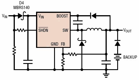
Figure 6: Output backup battery reverse discharge circuit when input short circuit is prevented
in conclusion
1 A suitable switching frequency ensures that the system has a sufficient input operating voltage range while minimizing the size and volume of the inductor and capacitor.
2 The actual maximum input operating voltage is determined by the minimum on-time required by the MOSFET. The actual minimum input operating voltage is determined by the minimum turn-off time required by the MOSFET.
3 The input transient voltage must be suppressed, the heat dissipation design should be checked, and the input short circuit and reverse connection protection circuit should be added to ensure the safe operation of the system.
This article refers to the address: http://
Components cost is the main cost of a PCBA project, normally 80-90% in massive PCB Assembly production. And with millions components types, it`s a tough job to do the Components Procurement (BOM Kitting) which need a experienced and effective team to manage it.
Done EMS service for 15years, we have a reliable components sourcing team and always can help our customers to get the new & original components in the quickest time at best prices. We ensure all parts are from standard supply chain. And we established good partnership with the major electronic components distributors like Digikey, Mouser, Farnell, RS, Arrow, Avnet, Future, etc.

Components Procurement
Components Procurement,Electronic Components Procurement,Procurement Electronic Component,PCB Components Procurement
ZhongFeng Electronic Technology Co., Limited , https://www.dopcba.com