
With the development of solid-state lighting technology, Group III nitride materials have attracted wide attention from researchers because of their stable material structure and the wavelength of light from ultraviolet to visible light.
GaN-based LEDs are typically grown on sapphire substrates by metal organic chemical vapor deposition (MOCVD). However, since the lattice mismatch between sapphire and GaN is as high as about 16%, a high dislocation density is formed in the GaN-based epitaxial layer, which seriously affects the performance of the GaN-based LED. The use of a patterned sapphire substrate can alleviate the stress caused by lattice mismatch in the gallium nitride-based epitaxial layer and effectively reduce the dislocation density, thereby obtaining a high-quality epitaxial layer, thereby improving the internal quantum efficiency [1]. . At the same time, the high-quality epitaxial layer can significantly reduce the heat generated during device operation and increase the lifetime of the LED. More importantly, for the conventional sapphire substrate GaN-based LED, due to the large refractive index difference between air and epitaxial layer (nGaN=2.5, n air=1), it is easy to form at the interface. Total reflection, so that only 4% of the light can exit the LED surface, and most of the light is confined inside the LED, eventually becoming heat loss, resulting in extremely low light extraction efficiency. Therefore, how to improve the light extraction efficiency of LED is one of the most practical research topics in the field of solid-state lighting, and the graphic sapphire substrate technology is currently the main method to solve the low efficiency of light extraction.
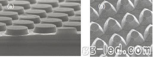
At present, the preparation techniques of the patterned substrate mainly include wet method and dry etching. The ICP dry etching technique [2] firstly applies a layer of photoresist on a sapphire substrate, uses a standard photolithography process to form a pattern on the photoresist, and then uses a photoresist as a mask, using BCl3, etc. The chemical gas is etched to produce a patterned sapphire substrate as shown in Figure 1(a).
The wet etching technique [3] is to deposit a SiO2 mask of about 100 nm thickness on a sapphire substrate by plasma enhanced chemical vapor deposition (PECVD), and to use a standard lithography technique to pattern the lithographic plate. Transfer to the SiO2 mask. Then, under the protection of the SiO2 mask, etching is performed using a mixed acid solution of sulfuric acid and phosphoric acid. Different etching times and solution concentrations affect the etching depth and etching angle of the sapphire substrate. Finally, the surface SiO2 mask was removed with a hydrofluoric acid solution to obtain a sapphire patterned substrate as shown in Fig. 1(b).
For more information, please refer to the March issue of "High-tech LED--Technology and Applications" magazine
Bbier's String Work Lights are manufactured with cable and molded plug and connector ends. String Work Lamp is available in 80 watt,100 watt,120 watt and 150 watt, each stringer comes with plastic or metal cages. The heavy duty construction is rated for outdoor use and is CE ROHS listed.
The Working Light is ideal for lighting workshops, garages and tight work areas. Led Work Lamp is designed to resist abrasions, moisture and sunlight. Its cage design protects the light bulb and makes it quick and easy to replace it when needed. String Work Lights can be mounted with a hook to be placed over work area. Led Work Light is ETL listed to be mounted near damp locations making it a great LED solution to light work areas, garage lighting, construction sites and many commercial and residential applications.

String Work Lights
String Work Lights,Led Work Lamp,String Work Lamp,Working Light
Shenzhen Bbier Lighting Co., Ltd , https://www.chinabbier.com