
1 Introduction
With the development of semiconductor technology, DSP performance continues to improve, and it is widely used in the fields of control, communication, and home appliances. The internal core component of the DSP, ALU, has a very high processing speed, while the speed of the external memory is relatively low. The storage system has become a bottleneck restricting the development of the DSP. This paper refers to the computer storage structure and uses the virtual storage technology to improve the structure of the storage system. The introduction of a secondary Cache memory structure in the DSP improves the working speed of the DSP under a small hardware overhead. This project was designed with high-performance low-power DSP cache to explore the structure and algorithm of the two-level cache.
2 cache overall design
The traditional memory is mainly composed of Dram, which works at a slower speed. The cache memory is mainly composed of SRAM. In the DSP, the storage system can be layered and divided into two parts: a smaller-capacity cache memory and a larger-capacity main memory, and the cache stores the more commonly used instructions and data consistent with the main memory. When the DSP performs an operation, it can first fetch instructions or data to a faster cache, and if it does not, access the instruction or data from the main. By increasing the hit rate of the cache, the overall running speed of the DSP can be greatly accelerated, thereby alleviating the bottleneck caused by the storage system.
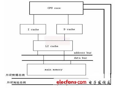
Figure 1 cache structure and interconnection diagram
Based on the above principles, we designed the overall structure of the DSP cache, as shown in Figure 1. The design uses a two-level cache design. The first-level cache uses a discrete structure, which separates the instruction cache from the data cache, so that the CPU can perform parallel operations on data and instructions, combined with DSP addressing, decoding, reading, and execution. The four-stage pipeline structure fully improves system efficiency. The secondary cache adopts a unified structure, and the data and the instructions share a cache. At this time, according to the specific situation of the program execution, the secondary cache automatically balances the load between the instructions and the data, thereby improving the hit rate. If the DSP does not find the required instructions and data in the level 1 cache, it can be found in the secondary cache. Under this structure, most of the data and instructions that cannot be found in the first level cache can be found in the secondary cache, which improves the hit rate of the entire cache system.
Increasing the capacity of the first-level cache can improve the hit rate, but as the cache capacity increases, the circuit structure will become complicated, the chip area and power consumption will increase, and the cache access time will become longer, thus affecting The speed to the ALU. Taking into account factors such as speed, area, power consumption, etc., we have set the capacity of the first-level instruction cache and data cache to 4KB.
The secondary cache is between the primary cache and the main memory. The access time is 3 to 4 ALU clock cycles, and its capacity is generally 4 to 8 times that of the primary cache. In the design, we set the capacity of the secondary cache to 32KB.
3 cache mapping and address structure
The mapping method used by the cache usually has three types: direct mapping, association mapping, and group association mapping. The direct mapping hit rate is low, and the jitter is easy to occur. Although the hit ratio is high, the circuit is complicated, the circuit complexity is complicated, and the hit rate is high. The group association mapping method is mainly used. In the group association mapping, the main storage space can be divided into blocks, the cache space is divided into groups, and one group contains multiple rows, and the size of the rows is equal to the size of the blocks. A particular block in main memory can only be mapped to a specific group in the cache, but can be mapped to different rows within the group. If j is used to represent the block number of the main memory, i is the group number in the cache, and m is the total number of lines in the cache. When the cache is divided into v groups, each group has k rows, the following relationship exists (see Equations 1, 2). ,
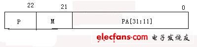
In the design, the secondary cache adopts a 4-way group associative structure, which is divided into a total of 256 groups, each group of 4 rows, each row of 8 32-bit units, and the total capacity is 32 KB. The cache's control logic simply divides the memory address into three fields: the tag field, the group number, and the word. In order to reduce the power consumption of the system, a scheme of separating the tag and the data body is adopted. In order to speed up the access speed, the block with the same line number in the cache is implemented in a data body. This cache can be divided into 4 tag memories, 4 data memories. Each tag memory can hold 256 tags, and each data bank has 256 rows of data. The division of the address is shown in Figure 2. The structure of the tag is shown in Figure 3.
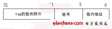
Figure 2 Address division of the secondary cache
Apple Macbook Battery,Macbook Battery
Shenzhen Aokal Technology Co., Ltd. , https://www.aokal.com