
0 Preface
With the rapid development of devices and processes, switch-type power converters have developed into high-efficiency and light-weight DC power supplies. Spacecraft (stars, arrows, ships, etc.) DC/DC converters (also known as secondary power supplies) also use this. Technology.
The main reason is that satellite electronic equipment is increasingly demanding the efficiency, weight, volume and reliability of the power supply, and the traditional linear power supply scheme can hardly meet the needs of the aircraft system. Among various types of DC/DC converters, PWM type DC/DC converters have been widely used due to their various types of structures, leading technology and easy implementation [1].
In a variety of topologies for switching power supplies in aerospace applications, switching power supplies for 100 V high-voltage bus input multiple outputs, most of which use two-stage converters, such as Buck+ push-pull two-stage converters, first pass Buck The circuit steps down the bus voltage, so that the bus voltage is subject to secondary adjustment, which reduces the voltage regulation rate. In terms of the number of components, the two-stage topology requires at least three power switches, and the power supply is bulky and the power density is low. The overall analysis is not very ideal; for a two-switch forward switching power supply that can withstand high-voltage input, the circuit structure is relatively simple, but it is not suitable for multi-output applications, the output cross-adjustment rate is low, and the stability is poor; The circuit topology suitable for small and medium power multi-output DC-DC converters is also a single-tube flyback circuit, which has a simple circuit structure and low cost, but the voltage of the main switch tube of the single-tube flyback circuit in a high input voltage occasion The stress is very high. The 200 V voltage MOSFET can not meet the requirements of Class I derating. If a higher voltage MOSFET is used, the on-resistance is higher. It will affect the power conversion efficiency, but also may cause the problem of low pressure discharge in a vacuum environment.
Therefore, in order to overcome the above mentioned problems, this paper designs a multi-output dual-tube flyback switching power supply based on UC1845 on the star, which is suitable for high voltage 100 V bus input and multi-output applications. For the double-tube flyback switching power supply, first of all, the circuit topology is simple, the input and output electrical isolation has a wide range of boost/buck, and has the advantages of automatic multi-output load equalization; secondly, due to the reliability requirements of the aerospace power supply, all devices must To meet the first-level derating standard, in the double-tube flyback converter circuit, when the power tube is turned off, the transformer leakage current can be fed back to the power supply through the freewheeling diode and the voltage across the switch tube is clamped to the power supply voltage, so the power The voltage stress and input voltage of the tube are equal, which expands the range of the selected tube and improves the reliability. Thirdly, the leakage inductance energy of the double-tube flyback switching power supply circuit can be fed back to the input side without adding any absorption circuit, so the conversion efficiency is also Higher than single-tube flyback circuits. Therefore, it is applied to the high-voltage input multi-output occasion of spacecraft, which has great advantages and has practical engineering application value.
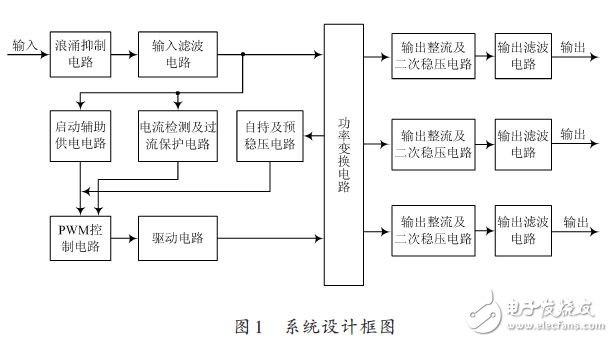
1 system design
The system design block diagram is shown in Figure 1.
2 double-tube flyback topology
The double-tube flyback topology is shown in Figure 2.
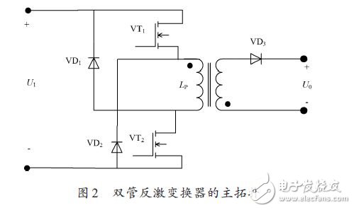
As shown in Figure 2, VT1 and VT2 are connected in series to the top and bottom of the transformer, respectively. The two switches are turned on and off at the same time. When they are turned on, all the primary and secondary names are positive. At this time, the secondary VD3 is reverse biased, the secondary has no current flowing, and the primary winding stores energy; when they are off At break, the current stored in the magnetizing inductance reverses the polarity of all winding voltages, VD3 is positively biased, and the energy stored in the magnetizing inductance is transmitted to the load. At this time, the potential of the same name terminal of LP is clamped to ground by diode VD2, LP The different terminal potential is clamped by the diode VD1 to the power supply voltage U1. Therefore, the source voltage of VT1 will not exceed U1, and the drain voltage of VT2 will not exceed U1. The leakage inductance spike is clamped, so that any switching transistor The maximum voltage stress does not exceed the maximum DC input voltage.
A significant advantage of the dual-tube flyback converter is that it does not have leakage inductance energy consumption. When the switch is turned on, all the energy stored in the leakage inductance is not consumed in the resistive element or the power switch tube, but is fed back to the U1 through the VT1 and VT2 when the switch is turned off. The leakage current is different from the LP. The name end flows out, flows into the positive pole of U1 through VD1, and then flows out from the negative pole, and returns to the same name end of LP through VD2, so that the leakage inductance energy can be fed back to the input side, which improves the conversion efficiency of the whole machine.
In the aerospace power supply, the dual-tube flyback switching power supply shows great advantages for the high-voltage 100 V bus input power supply.
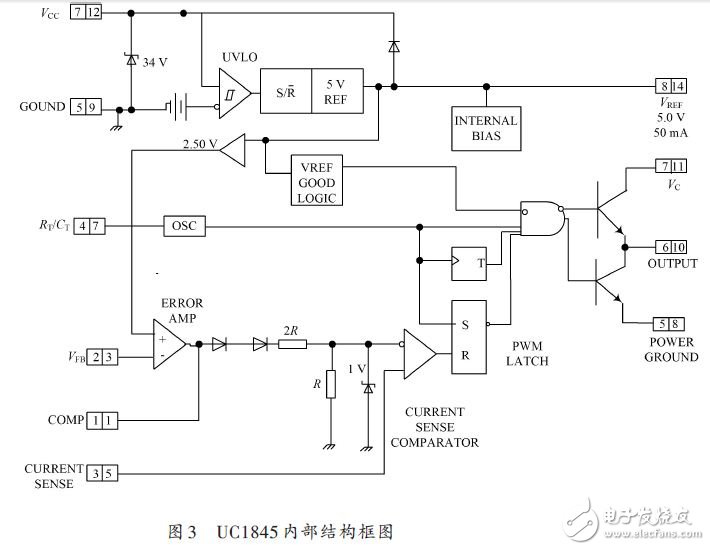
3 UC1845 control circuit
The UC1845 is a current-controlled PWM controller manufactured by Texas Instruments. The circuit has an adjustable switching frequency, current feedback and voltage feedback dual-loop control, and high voltage regulation and load regulation. The block diagram of its internal function module is shown in Figure 3. In Figure 3, UC1845 mainly includes:
5.0 V reference, high gain error amplifier, current comparator, RS flip-flop and undervoltage lockout power supply circuit. The pin functions of the UC1845 chip with 8-pin package are as follows: pin l is the error amplifier output for loop compensation; pin 2 is the inverting input of the error amplifier, usually connected to the switching power supply output through a resistor divider. Voltage feedback, adjust the duty cycle of the output to stabilize the output voltage; pin 3 is the current sampling pin, the pulse width modulator uses this information to terminate the conduction of the output switch, protect the switch tube to avoid overcurrent damage; At timing, through time resistor RT, connected to reference output pin 8 and time capacitor CT connected to ground, the oscillator frequency and maximum output duty cycle are adjustable, the oscillation frequency is f=1.72 (RTCT); foot 5 is control The common ground of the circuit and the power supply; the foot 6 is the square wave pin of the output drive switch. For the totem pole output, it can directly drive the gate of the power tube MOSFET; the foot 7 is the positive power supply (VCC) of the control IC. The startup voltage is 8.4 V, and the maximum output current can reach 1 A. It is suitable for driving MOSFET and suitable for medium and small power. DC/DC switching power supply; pin 8 is the internal reference voltage source to generate a 5.0 V reference voltage. As the internal power supply of the UC1845, it is attenuated by 2.5 V as a reference for the comparison amplifier and can be used as a power supply for 5 V/50 mA to the external circuit. . The UC1845 also includes an overvoltage and undervoltage protection circuit that stops when the supply voltage drops below 7.6V.
With a high operating temperature range, the UC1845 can operate stably from -65 to 150 °C for aerospace applications [3].
4 main circuit design
The main circuit adopts the double-tube flyback circuit as the overall system frame. The UC1845 chip and the corresponding peripheral circuit form the PWM controller. The feedback circuit adopts magnetic isolation feedback, realizes multiple output through one feedback control quantity, and cooperates with the output end. The low dropout three-terminal regulator can improve the stability of each output load.
Hanukah candle /Chanukah Candle/Jewish candles for holiday use .small Spiral Candle and taper candles color popular in America and Isreal market .
there are 6 color in box , yellow red white green blue orannge color as your require ,
3.8gram/pc multi-color candle 44pcs/box 50box/ctn
7gram/pc multi-color candle 45pcs/pvc box 25box/ctn
shipment is very quickly ,in the 30days after get the depsoit .welcome to visit my factory
pls be free to contact with me .
Chanukah Candle
Chanukah Candle,Hand-Dipped Chanukah Candle,Colorful Chanukah Candles,Chanukah Candle Kits
Shijiazhuang Zhongya Candle Co,. Ltd. , https://www.zycandlefactory.com