
Just as wireless operators are scrambling to provide new services, new equipment, and increased bandwidth and business solutions to improve their profitability, infrastructure companies are racing to put the 5G equipment that forms the foundation of next-generation wireless communications into practical use. To make this 5G wireless infrastructure a reality, BEEcube, recently acquired by National Instruments, is using the FPGA and Zynq®-7000 All Programmable SoC to provide new simulation systems and mobile handset emulators for 5G device manufacturers. BEE7 and nanoBEE are driving the design team's innovation and productivity so they can bring 5G technology to market ahead of their competitors.
Before we dive into the new BEEcube FPGA-based products, let's briefly introduce the wireless communications industry's vision for the 5G market and the technical challenges facing the market.
5G vision
A key part of building the future of the wireless industry is the massive deployment of 5G wireless networks. The primary goal of 5G is to support thousands of capacity growth, support the connection needs of at least 100 billion devices, and provide 10Gbps data rates for individual users. In addition, these new networks provide large-scale, low-latency connections between people, machines, and devices. The 5G network is expected to be deployed from 2020. By evolving existing wireless radio access technologies such as LTE and Wi-Fi, combined with new technologies, 5G wireless access technologies can be created.
Although the industry has set the ultimate goal of 5G, how to achieve these goals is a problem that needs to be invested in billions of dollars. Many companies around the world are developing 5G infrastructure equipment and a large number of advanced equipment that communicates via 5G.
Although the detailed technical solutions of 5G have not yet been determined, there are a few things that are very clear. Future wireless systems will leverage the spatial diversity provided by massive MIMO, as well as beamforming and related technologies to more efficiently leverage existing bandwidth. The newly allocated spectrum will be dedicated to cellular communications, increasing overall channel capacity. Higher carrier throughput will be achieved through carrier aggregation technology and new frequency bands. The density of urban cellular sites will increase, while power consumption requirements will decrease, and spectrum utilization in a given area will also increase significantly. The core network will increase the use of the cloud for data and control.
Since the 5G standard has not yet been developed, if a company can use a powerful FPGA platform with massive I/O to demonstrate a functioning "wireless" system, it will help its ideas and specifications be adopted by international standards organizations. These platforms enable rapid prototyping, making it easy to use real-world data test algorithms in the field and run continuously for days or weeks.
The ideal wireless infrastructure prototyping platform
There is no single platform that meets all the requirements for 5G prototyping. But it has been able to clarify the key requirements.
A 1,000-fold increase in data throughput puts pressure on all 5G communications hardware. The capacity density of all prototype platforms must be scalable to tens of terabytes, access to hundreds of fibers, and support RF analog data for dozens of GS.
The DSP processing power required to implement high-order modulation schemes on many antennas and sectors used in massive MIMO is extremely high. Tens of thousands of multiply accumulator (MAC) units are required.
As new communication systems become more complex, not all OEMs retain all of their IP, except for the largest OEMs. Having a rich IP set including massive MIMO, CPRI, multi-waveform and LTE-Advanced protocol stacks can significantly accelerate the development process (see sidebar).
Operators around the world are working hard to push as much processing as possible to the cloud. This effort can take advantage of the economies of scale of the data center and, by doing so, reduce the processing cost per call. Efficient connectivity to the cloud requires a 10GE, 40GE or PCIe® interface.
The programming model must support existing major C languages, C-to-logic gates, VHDL, Verilog design flows, and various advanced modeling environments (LabVIEW and MATLAB®/Simulink® are the two most common).
In terms of clocks, in order to maintain the integrity of broadband information signals with high information density, the hardware must be able to extract embedded clocks from CPRI or synchronous Ethernet, while also being able to clear the clock and make the device at an ADC sampling frequency of up to 6 GHz. The rack keeps the clock jitter below 300fs.
To meet these challenges, BEEcube has developed a powerful new simulation platform called BEE7. The platform leverages the industry-leading features of Xilinx Virtex®-7 FPGAs.
BEE7 platform architecture
The BEE7 platform is a new high-end architecture designed by BEEcube to meet the requirements of the above-mentioned next-generation communication system. Below we will detail BEE7 and learn how to solve 5G prototyping problems with one platform.
One of the biggest challenges you face when developing advanced wireless prototyping architectures is connectivity. The amount of data that needs to be transferred quickly and efficiently is extremely large. At the heart of the BEE7 prototyping system is the Xilinx XC7VX690T. Combining 80 serial transceivers with 3,600 DSP slices, the 690T is the world's leading engine for advanced wireless applications (both for prototypes and for early field trials).
Figure 1 shows the BEE7 blade. Note: The ATCA form factor is typically used in the telecommunications industry. This makes it easy to use BEE7 in existing base station boxes for field trials. The four 690T FPGAs are connected in the manner shown in Figure 2. Four FMC slots connect each FPGA to a high-performance analog card that supports a sampling rate of 5.6Gsps. A 64GB total DDR3 memory can be used to collect data as well as a buffer for broadcast data. This memory is extremely useful in the early stages of prototyping. The design team can use LabVIEW from National Instruments or MATLAB from The Mathworks to create simulation vectors, then download them to system memory for playback, or perform detailed analysis of the acquired data.
Serial transceivers in 690T devices are rated at 13.1Gbps. Many of the standards used in telecommunications are centered around 10Gpbs, such as 10 Gigabit Ethernet and CPRI (interface rate: 8), which is a performance indicator we use in BEE7. In this way, each FPGA can provide a connection rate of 800 Gbps, as shown in Figure 2.
Below we introduce the specific aspects of the BEE7 prototyping environment and some of the trade-offs and design decisions that need to be made during the design process.
Point-to-point connection
One of the goals of the BEE7 architecture is to provide the lowest possible data stream latency and guaranteed stream throughput. These goals are simply not possible with a shared bus architecture because different customers on the bus connect to the bus at any given time, increasing latency and interfering with the real flow environment used by other users. Therefore, BEE7 uses a point-to-point connection model instead.
The high speed serial deserializer is the backbone of data transmission in the BEE7 environment. By carefully tuning PCB trace width, dielectric material thickness, via layout and size, point-to-point 100 ohm transmission lines are available to ensure optimum performance and signal integrity. In many cases, high-performance traces are buried in the inner panel to reduce EMI emissions and are easier to pass CE certification or FCC approval.
Connections from BEE7 blades to other devices, including other BEE7 blades, can be divided into three categories: shorter than three meters, over 300 meters, and in between.
For links shorter than three meters, copper connections can be used, and this is definitely the lowest cost alternative. Use SFP+ or QSFP connectors with a short jumper cable for use in a BEE7 environment, and it is recommended to use a blade in one equipment rack to communicate with the blade. For longer distances up to 300 meters, short-range optical communications offer the most cost-effective alternative. The BEE7 has a built-in short-range optical module. Figure 2 shows that each FPGA has 12 serial deserializer channels connected to the inter-module optical transceiver (iMOT). These interfaces are placed on the front of the BEE7 blade for direct connection to the adjacent remote radio unit (RRH) via the Common Public Radio Interface (CPRI).
Longer distances require special long-haul optical transceivers. This transceiver can transmit distances up to 40 kilometers without the use of repeaters. These transceivers can be easily plugged into the SFP+ and QSFP connectors of the Back End Conversion Module (RTM) for RRHs over 300 meters from BEE7.
The total connection speed from RTM to BEE7 ATCA blades is 640Gbps; the total connection speed from the front-end iMOT connector to the BEE7 ATCA blade is 480Gbps. If analog I/O is not required, an additional FW card can be used to provide an additional 320 Gbps.
Common challenges in designing serial deserializers include how to solve problems such as delay, calibration, and timing. BEEcube's BPS software automates calibration at startup and abstracts most of the underlying details of the serial deserializer. This design of the serial deserializer in BEEcube is relatively straightforward, as the latency characteristics of each multi-gigabit transceiver (MGT) are similar to FIFO.
Timing problem
In a distributed system, if the clock and data are transmitted separately, it will be difficult to transmit over long distances. Standards such as CPRI are specifications for transmitting data from remote radio units to baseband processing units in the wireless world. A recovered embedded clock (such as in CPRI) generally has poor phase noise characteristics. The BEE7 PLL-based special circuit reduces this phase noise below 300fs. These clocks are multiplied to generate a GHz-level sample clock while maintaining phase noise below 300fs.
Flexible clocks can be assigned to analog FMC cards (most critical to the sampling clock) and FPGAs.
RF considerations
Direct RF sampling and synthesis up to 6 GHz has long been a development goal for software-defined wireless, but until recently the availability of high-speed DACs and ADCs was realized. BEEcube has developed a modular architecture that supports high-performance analog interfaces via FMC cards connected to the motherboard.
Modules with sampling rates up to 5.6Gsps are available now, allowing the 2GHz spectrum to be directly integrated or digitized and transferred back and forth between the module and the FPGA board to meet modulation/demodulation and other processing requirements. The analog FMC card supports the first and second Nyquist domains, so the user can verify the entire spectrum below 2 GHz or the 2 GHz spectrum block in the higher frequency range.
High-speed DACs and ADCs are extremely difficult to integrate effectively into real-world systems. They use a staggered layout for maximum performance while requiring an extremely stable clock with clock jitter of less than 500fs. With a 307.2MHz reference clock, the typical clock jitter provided by the BEE7 platform is less than 300fs when the measured phase noise distribution is in the range of 100Hz to 10MHz. These DACs and ADCs also require a special training sequence that sets the phase of the data strobe signal to maximum data integrity when pushing data to or from high speed devices. BEEcube's platform completes all training sequences on the first launch of the board. So developers don't need to pay attention to these low-level details to achieve "out of the box" operations.
Design flow and IP
C/C++, MATLAB, VHDL, Verilog, LabVIEW, and Simulink all play a role in the development of next-generation 5G designs. The BEEcube platform has always been designed to be tool-independent, allowing designers to use any design process they prefer. When all the basic problems are solved from the perspective of tool flow, the focus is quickly turned to IP.
BEEcube provides a number of necessary low-level interfaces for building high-performance communication designs. While Xilinx supports CRPI and PCIe, BEEcube offers 10Gb and 1Gb Ethernet cores, combined with a Xilinx Aurora kernel synchronization version for inter-FPGA communication. In addition, an interface to the onboard DDR memory is provided along with standard FIFO and block RAM interfaces.
Advanced IP blocks are a powerful way to speed up the design process. This is discussed in detail in the sidebar.
nanoBEE--User Equipment Solutions
BEE7 provides the massive connectivity and DSP processing power required for infrastructure solutions. Is there a tool that can emulate a handheld terminal (or user equipment (UE) in the industry terminology?) A handheld terminal requires moderate DSP processing power and connectivity, and is likely to run on battery in mobile testing with a highly integrated MAC and Built-in higher layer protocol processing capabilities.
The physical layer of 5G user equipment must be highly flexible and challenging for any typical processor architecture, but for the 2,020 DSP slices in the Zynq 7100 device, the physical layer is very simple and intuitive. Implementing 10Gbps user equipment connectivity in the Zynq 7100 SoC is also relatively straightforward.
The two A9 ARM® cores in the Zynq family make them ideal for user device emulators. These two cores implement MAC and a higher protocol layer. Most existing mobile phones use ARM processors, so companies can reuse a large number of existing code bases for higher-level processing. Tight integration of the ARM core and programmable architecture maintains low latency and improves performance. Keeping the power consumption of the Zynq SoC and other nanoBEE hardware below 5w means that you can power the product with a battery pack, which is definitely good for testing user device emulators.
nanoBEE uses the same power amplifiers, diplexers, input filters, and other signal chain components to provide operation over most LTE-A bands and in the unlicensed 2.4 GHz and 5 GHz bands while complying with 3GPP protocol standards User device emulator.
The nanoBEE shown in Figure 3 took less than 18 months from concept to product launch.
Looking forward to five years
Numerous 5G technology challenges are in full swing. We are still five years away from commercial use, but as standards become fixed, many companies need to prototype these emerging algorithms and applications. Combining Xilinx FPGAs and Zynq SoC devices with commercial 5G prototyping platforms from companies such as BEEtube can save significant development time compared to custom prototyping platforms. These tools allow system architects and designers to focus on finding the best architecture and algorithms, rather than focusing on the architectural design of the design platform. These tools also enable telecom operators to accelerate early trials and gain experience with new systems, algorithms and network architectures.
Based on our vision for widespread deployment of 5G in 2020, it is likely that most OEMs will sell production equipment based on Xilinx FPGAs and All Programmable SoCs. The hardware complexity of the 5G physical layer is difficult to ensure that the ASIC implementation does not have hardware defects and is flexible enough to meet evolving standards. Making hardware “soften†is the smart choice for the smartest OEMs.
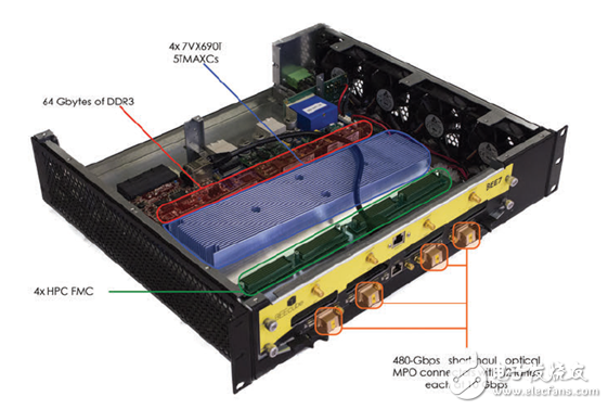
Figure 1: BEE7 blades on an ATCA rack for prototyping and field testing of the most demanding 5G wireless applications, including C-RAN, massive MIMO, and millimeter waves. 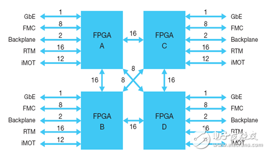
Figure 2: This BEE7 interconnect architecture diagram shows the number of 10Gbps channels. The total serial transceiver connection rate per FPGA is 800Gbps. 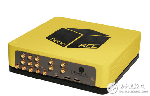
Figure 3: nanoBEE is a terminal emulation system designed to accelerate the development of next-generation wireless products.
IP accelerates 5G development approach
The 5G wireless standardization process is tortuous, and any company that wants to develop 5G completely needs to invest a lot of money. Companies can work with vendors that already have a wealth of must-have IP to accelerate 5G development efforts.
What type of IP can speed up this work? At the most basic level, IPs such as 10GE, CPRI, and DDR are indispensable for any high-performance wireless system. Along this chain, any 5G system must support legacy LTE-A systems, and the basic LTE-A protocol stack is still essential. This was followed by IP for different 5G research areas, including air interface waveforms, massive MIMO, millimeter waves, and C-RAN.
New air interface waveforms include GFDM, UFDM, FBMC, and more. These waveforms are primarily used to improve spectral efficiency and power consumption characteristics. The OFMDA used in LTE-A has a high peak/average power ratio, so expensive circuitry is required to keep the power amplifier linear, reducing out-of-band interference and intermodulation distortion.
Millimeter waves require different channel model estimates because of the different propagation characteristics at these frequencies. IP must target very high bandwidth (up to 5 GHz) and the attendant high peak data rate.
Only available IP is not enough. Users must be able to easily connect IPs together. National Instruments provides IPs that are carefully selected to run on multiple types of FPGAs and processors and provide a library focused on 5G prototyping. The IP is easily connected in the LabVIEW Communication System Design Suite from National Instruments. LabVIEW also provides all the waveform source files and analysis tools needed to motivate and analyze your design.
LabVIEW plus a variety of IP libraries saves months of development time. In addition, the selected IP works fine. LabVIEW seamlessly interacts with the Xilinx toolchain for quick exploration and experimentation. Combined with the various hardware levels offered by National Instruments, this is the fastest way to achieve an effective 5G communication design prototype. It is worth mentioning that BEEcube, now a subsidiary of National Instruments, will provide LabVIEW support for its hardware in the near future.
Swimming Pool Lighting Led Driver
For the water under the lamp products, the water level is very high, IP68 grade Led Driver, the general low pressure is better, high voltage to avoid leakage risk, generally DC12V / 24V based.
A comprehensive range of IP Rated/Waterproof AC/DC LED lighting power supplies suitable for use in a range of Lighting applications, including Architectural Lighting, Task Lighting, Medical Lighting, Transportation Lighting, Entertainment Lighting, Moving Signs, Safety & Security Lighting and Outdoor Area Lighting Applications. LED Lighting power supplies, Halogen Lighting Power Supplies & LED Drivers in constant voltage or Constant Current models and IP64, IP65, IP66 or IP67 rated.

What's the benefits of Fahold Driver?
- Standard Linear Lighting
- Cost-effective led driver solution for industry,commercial and other applications
- Good quality of led driver with high efficiency output to meet different requirements
- Easy to order and install,requiring less time,reducing packaging waste and complexity
- Flexible solution
FAQ:
Question 1:Are you a factory or a trading company?
Answer: We are a factory.
Question 2: Payment term?
Answer: 30% TT deposit + 70% TT before shipment,50% TT deposit + 50% LC balance, Flexible payment
can be negotiated.
Question 3: What's the main business of Fahold?
Answer: Fahold focused on LED controllers and dimmers from 2010. We have 28 engineers who dedicated themselves to researching and developing LED controlling and dimming system.
Question 4: What Fahold will do if we have problems after receiving your products?
Answer: Our products have been strictly inspected before shipping. Once you receive the products you are not satisfied, please feel free to contact us in time, we will do our best to solve any of your problems with our good after-sale service.
Swimming Pool Lighting Led Driver
230Vac To 24Vdc Power Supply,Led Street Lighting,Led Street Lamp Ip67 Driver
ShenZhen Fahold Electronic Limited , https://www.fahold.com