
introduction
Multi-voltage electronic systems often require complex power supply voltage tracking or sequencing. Failure to meet this requirement can result in system errors or even permanent failures at the site of use. The design challenges encountered in meeting these requirements are often found in distributed power architectures where point-of-load (POL) DC/DC converters or linear voltage regulators are scattered in the PC board space, sometimes in different locations. Circuit board on the plane. The problem is that in the layout of the circuit board, the power circuit is often the last designed circuit. Therefore, no matter how small the remaining circuit board area is, you have to put it in hard. A simple, pin-compatible, flexible solution is often required to meet these requirements.
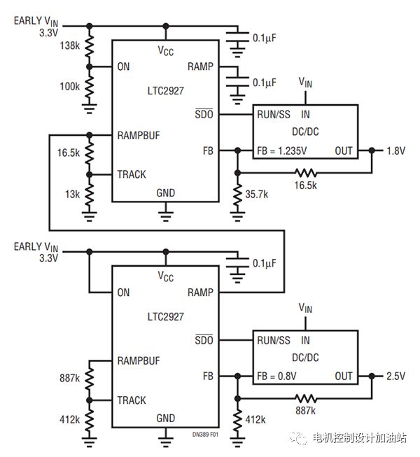
Figure 1: Dual Channel Power Supply Tracking Application
The LTC®2927 provides a simple and versatile solution for tracking and sequencing, with a tiny footprint and without the drawbacks of using series MOSFETs. In addition, since the LTC2927 can regulate the output voltage of the regulator without changing the dynamic characteristics of the power control loop, the stability and transient response performance of the power supply will not be affected.
Basic operation
As shown in Figure 1, for each POL converter that must be tracked or sequenced, an LTC2927 can be placed at the load point. By selecting several resistors and one capacitor, one power supply can be configured to ramp up and ramp down in multiple voltage modes. With the choice of resistors, a slave power supply can track the master signal accurately or with a different ramp rate, voltage offset, delay, or a combination of these different combinations.
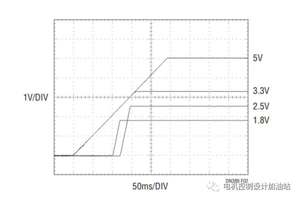
Figure 2: Used to illustrate tracking, sequencing, and ramp rate control
A four-power system output curve
Figure 2 shows a quad power trace and sequencing curve that highlights the flexibility the LTC2927 has. A master signal is generated by connecting a capacitor between the RAMP pin and ground or providing another ramp signal to be tracked. The ramp signal can be a master signal generated by another LTC2927 or another tracking controller (eg, LTC2923). Similarly, another supply voltage can also be used as a master signal. If an external ramp signal is used, it can be connected directly to the RAMP pin or to a resistive divider connected to the TRACK pin.
The LTC2927 provides an SDO output for applications that require slave power down or master control of the RUN/SS pin. SDO will be pulled low when the ON pin voltage is less than 1.23V and the RAMP pin voltage is less than 200mV.
Negative power supply tracking
The LTC2927 can also be used to track negative voltage regulators. Figure 3 shows a trace example using a LT3462 negative output DC/DC converter to generate a –5V supply. The converter has a ground-based reference that allows it to sink current from a node that divides the RFA. In order to properly sink current from the LT3462's FB network, a current mirror must be placed between the LTC2927 and the converter. Figure 4 shows the trace of the circuit in Figure 3 (using a ramp rate of 100V/s). VMASTER is positive, but for the sake of clarity, the negative values ​​are given in the figure. With VMASTER = 0V, the -5V slave supply will not be pulled up to 0V because the ground-referenced current mirror cannot pull its output all the way to ground. If the converter has a FB reference voltage higher than 0V, or there is a negative supply available for the current mirror, the voltage offset can be removed. Figure 5 shows the final waveform.
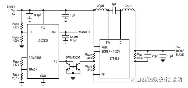
Figure 3: Power trace of a negative voltage regulator referenced to GND
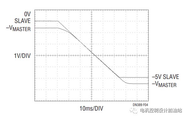
Figure 4: Achilles curve of the application circuit of the negative voltage regulator shown in Figure 3

Figure 5: Achilles trace of negative voltage regulator application circuit (without current mirror pull-down limit)
in conclusion
The LTC2927 simplifies power tracking and sequencing by providing superior performance within a tiny point-of-load footprint. With a small number of resistors, simple or complex power features can be configured. Excluding the series MOSFET, its parasitic voltage drop and power dissipation are also eliminated. The LTC2927 integrates all of these features in the tiny 8-lead ThinSOTTM and 8-pin (3mm x 2mm) DFN packages.
Saintish all in one off grid inverter comes with two output modes: mains bypass and inverter output to achieve uninterrupted power supply function. and the solar off grid inverters are available in 4 charging modes: Only Solar, Mains Priority, Solar Priority and Mains & Solar hybrid charging.
It adopts full digital voltage/current double closed-loop control and advanced SPWM technology to achieve output pure sine wave. Our solar inverter equips advanced MPPT technology, with efficiency up to 99.9% and wide MPPT voltage range.
There is function of activating lithium battery with solar energy and AC mains power, it also supports connection of lead-acid battery and lithium battery.
The LCD screen designed and 3 LED indicator lights dynamically display system data andoperation states.
ON/OFF rocker switch can control AC output.
With power saving mode function, it can reduce no-load loss.

All In One Inverter, All In One Off Grid Inverter, Hybrid Inverter, Off Grid Energy Storage
Hangzhou Saintish Technology Co.,Ltd. , https://www.saintishtech.com